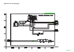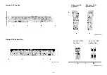
WAVEFORMS
LC6WF
9-1
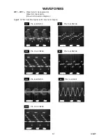
Input:
NTSC Color Bar Signal (with 1kHz Audio Signal)
WF1 ~ WF7 =
Waveforms to be observed at
Waveform check points.
(Shown in Schematic Diagram.)
CVBS
0.2V
20
µ
s
WF1
Pin 6 of CN703
S-VIDEO-Y
0.2V
WF2
Pin 10 of CN703
20
µ
s
S-VIDEO-C
0.2V
WF3
Pin 8 of CN703
20
µ
s
AUDIO
0.1V
0.5ms
WF7
Pin 14 of IC801
COMP-Pr
0.2V
20
µ
s
Pin 14 of CN703
WF6
COMP-Pb
0.2V
20
µ
s
Pin 15 of CN703
WF5
COMP-Y
0.2V
20
µ
s
Pin 12 of CN703
WF4
Summary of Contents for SLC195EM8
Page 35: ...8 6 A81N5SCM4 Main 4 5 Schematic Diagram ...
Page 37: ...8 8 A81N5SCF Function Junction Schematic Diagram ...
Page 38: ...8 9 A81N5SCIR IR Sensor Junction Schematic Diagram ...
Page 39: ...8 10 A81N5SCD1 DTV Module 1 2 Schematic Diagram ...
Page 40: ...8 11 A81N5SCD2 DTV Module 2 2 Schematic Diagram ...
Page 41: ...8 12 A81N5SCDM1 Digital Main 1 6 Schematic Diagram ...
Page 46: ...8 17 A81N5SCDM6 Digital Main 6 6 Schematic Diagram ...


