background image

8-18

BA81N0F01022-1

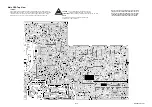
Main CBA Top View

Because a hot chassis ground is present in the power
supply circuit, an isolation transformer must be used.
Also, in order to have the ability to increase the input
slowly,when troubleshooting this type power supply
circuit, a variable isolation transformer is required. 

For continued protection against risk of fire, 
replace only with same type  4 A, 125V fuse.

CAUTION ! :

ATTENTION : 

Utiliser un fusible de rechange de m

ê

me type de  4A, 125V.

4A/125V

CAUTION !

Fixed voltage (or Auto voltage selectable) power supply circuit is used in this unit.
If Main Fuse (F601) is blown , check to see that all components in the power supply
circuit are not defective before you connect the AC plug to the AC power supply.
Otherwise it may cause some components in the power supply circuit to fail.  

NOTE:

The voltage for parts in hot circuit is measured using
hot GND as a common terminal.

Summary of Contents for SLC195EM8

Page 1: ...LC195EM8 2 and the original model SLC195EM8 All other information is described in the service manual of the model SLC195EM8 TM EMERSON AND THE G CLEF LOGO ARE REGISTERED TRADEMARKS OF EMERSON RADIO CORP PARSIPPANY NEW JERSEY U S A 19 COLOR LCD TELEVISION SLC195EM8 2 SUPPLEMENT ...

Page 2: ...of this manual or any revision hereto is strictly prohibited Information in this document is subject to change without notice Funai reserves the right to change the content herein without the obligation to notify any person or organization of such changes with the design is a registered trademark of Funai Electric Co Ltd and may not be used in any way without the express written consent of Funai A...

Page 3: ...SERVICE MANUAL TM EMERSON AND THE G CLEF LOGO ARE REGISTERED TRADEMARKS OF EMERSON RADIO CORP PARSIPPANY NEW JERSEY U S A 19 COLOR LCD TELEVISION SLC195EM8 ...

Page 4: ... service might be done or of the possible hazardous consequences of each way Consequently Funai has not undertaken any such broad evaluation Accordingly a servicer who uses a service procedure or tool which is not recommended by Funai must first use all precautions thoroughly so that neither his safety nor the safe operation of the equipment will be jeopardized by the service method selected TABLE...

Page 5: ...d Freq Range 28dBm kHz 100 2 ATSC Dynamic Range min max ch 4 ch 10 ch 41 dBm dBm dBm 76 0 76 0 74 4 Description Condition Unit Nominal Limit 1 Native Pixel Resolusion Horizontal Vertical pixels pixels 1440 900 2 Brightness w filter cd m2 250 3 Viewing Angle Horizontal Vertical 75 to 75 70 to 70 Description Condition Unit Nominal Limit 1 Over Scan Horizontal Vertical 5 5 2 Color Temperature x y K 1...

Page 6: ...ed and some may drop slightly below these specifications Limit specifications represent the absolute worst condition that still might be considered acceptable In no case should a unit fail to meet limit specifications Description Condition Unit Nominal Limit 1 Audio Output Power 10 THD Lch Rch W 1 0 1 0 0 9 0 9 2 Audio Distortion 500mW Lch Rch 0 5 0 5 2 0 2 0 3 Audio Freq Response NTSC 6dB Lch 6dB...

Page 7: ...om any AC source connect an electrical jumper across the two AC plug prongs Place the instrument AC switch in the on position Connect one lead of an ohmmeter to the AC plug prongs tied together and touch the other ohmmeter lead in turn to each tuner antenna input exposed terminal screw and if applicable to the coaxial connector If the measured resistance is less than 1 0 megohm or greater than 5 2...

Page 8: ...m is not isolated from the AC power line The two ground systems are electrically separated by insulation material that must not be defeated or altered 5 Observe original lead dress Take extra care to assure correct lead dress in the following areas a near sharp edges b near thermally hot parts be sure that leads and components do not touch thermally hot parts c the AC supply d high voltage and e a...

Page 9: ... PVC tubing 3 Spacers 4 Insulators for transistors E When replacing AC primary side components transformers power cord etc wrap ends of wires securely about the terminals before soldering F Observe that the wires do not contact heat producing parts heat sinks oxide metal film resistors fusible resistors etc G Check that replaced wires do not contact sharp edged or pointed parts H When a power cord...

Page 10: ...exposed accessible parts RF terminals antenna terminals video and audio input and output terminals microphone jacks earphone jacks etc is lower than or equal to the specified value in the table below Measuring Method Power ON Insert load Z between B earth ground power cord plug prongs and exposed accessible parts Use an AC voltmeter to measure across both terminals of load Z See Fig 2 and followin...

Page 11: ...the Flat Pack IC about 5 to 6 seconds Fig S 1 1 2 Remove the flat pack IC with tweezers while applying the hot air 3 Bottom of the flat pack IC is fixed with glue to the CBA when removing entire flat pack IC first apply soldering iron to center of the flat pack IC and heat up Then remove glue will be melted Fig S 1 6 4 Release the flat pack IC from the CBA using tweezers Fig S 1 6 CAUTION 1 The Fl...

Page 12: ...y one using a sharp pin or wire to which solder will not adhere iron wire When heating the pins use a fine tip soldering iron or a hot air desoldering machine Fig S 1 4 3 Bottom of the flat pack IC is fixed with glue to the CBA when removing entire flat pack IC first apply soldering iron to center of the flat pack IC and heat up Then remove glue will be melted Fig S 1 6 4 Release the flat pack IC ...

Page 13: ...s Fig S 1 6 Note When using a soldering iron care must be taken to ensure that the flat pack IC is not being held by glue When the flat pack IC is removed from the CBA handle it gently because it may be damaged if force is applied 2 Installation 1 Using desoldering braid remove the solder from the foil of each pin of the flat pack IC on the CBA so you can install a replacement flat pack IC more ea...

Page 14: ...d to remove any static electricity that may be charged on the body 2 Ground for Workbench Be sure to place a conductive sheet or copper plate with proper grounding 1 MΩ on the workbench or other surface where the semi conductors are to be placed Because the static electricity charge on clothing will not escape through the body grounding band be careful to avoid contacting semi conductors with your...

Page 15: ... L 2 5 Refer to the following Reference Notes in the Table Step Loc No Part Removal Fig No Remove Unhook Unlock Release Unplug Unclamp Desolder Note 1 Arm Assembly D1 2 S 1 4 S 2 2 Stand Cover D1 3 Rear Cabinet D1 8 S 3 4 Junction CBA D2 D3 CN705 CN706 WH1101B WH1151B 5 Function CBA D2 D3 3 S 4 6 IR Sensor CBA D2 D3 2 S 5 7 Jack Holder D D2 2 S 6 2 S 7 2 Stand Cover 7 Jack Holder D 3 Rear Cabinet ...

Page 16: ...4 2 A81N5DC Fig D1 3 Rear Cabinet S 1 S 3 1 Arm Assembly 2 Stand Cover S 2 S 3 S 3 S 3 S 3 S 2 ...

Page 17: ... CBA 15 Front Cabinet 14 Speaker 14 Speaker 12 Tilt Stand Holder S 9 S 11 11 Main CBA S 7 S 6 10 DTV Module CBA Unit Module PCB Holder 13 LCD Module S 12 S 8 S 10 S 10 S 10 S 12 S 12 S 12 S 12 S 12 S 4 S 10 S 10 8 Digital Main CBA Unit S 5 S 13 S 13 4 Junction CBA Fig D2 ...

Page 18: ...N1502 CN1503 CN1504 CN1901 CN1902 Digital Main CBA Unit To LCD Module CN61 To Speaker DTV Module CBA Unit CN101 CN102 CN802A AC CORD CN401 CN402 To LCD Module To Speaker CN801A CN705 CN706 CN1102 CN1152 WH1101B WH1151B Junction CBA WH1101 Function CBA WH1151 IR Sensor CBA Fig D3 ...

Page 19: ...control unit 4 Color Analyzer How to make the Service remote control unit Cut A portion of the attached remote control unit as shown in Fig 1 How to set up the service mode Service mode 1 Use the service remote control unit 2 Turn the power on 3 Press the service button on the service remote control unit as shown in Fig 1 1 Purity Check Mode This mode cycles through full screen displays of red gre...

Page 20: ... If this adjustment is incorrect PC signals do not reproduce the corresponding color 1 Input XGA 100 White signal 2 Enter the service mode 3 To enter the Auto Calibration adjustment mode press 6 button on service the remote control unit 4 To start auto adjustment press 3 button on the service remote control unit In the auto adjustment mode Please wait appears on the screen Upon completion OK appea...

Page 21: ...o the CHROMA mode and bring the optical receptor to the center on the LCD Panel surface after zero point calibration as shown above Note The optical receptor must be set perpendicularly to the LCD Panel surface 4 Enter the Service mode Press VOL n button on the service remote control unit and select C D2 mode 5 CUTOFF Press 1 button to select COR for Red Cutoff adjustment Press 3 button to select ...

Page 22: ...ce button on the service remote control unit Refer to page 5 1 To cancel the service mode press POWER button on the service remote control unit 3 Press DISPLAY button on the service remote control unit to initialize the LCD television 4 FF will appear in the upper left of the screen FF color will change to red from white when initialzing is complete ...

Page 23: ... CN1502 PROTECT 5 2 22 BACKLIGHT SW 20 4 BACKLIGHT ADJ 21 3 INPUT 2 20 4 CN704 IF MUTE 23 1 DTV ON H 3 21 CN1504 CN703 AUDIO MUTE 21 3 VOLUME 20 4 CN1503 INPUT 1 19 5 S SW 11 13 INPUT 0 18 6 AFT IN 22 2 FSC 16 8 SCL 13 11 SDA 15 9 P ON H1 4 4 SDA SCL BACKLIGHT ADJ TO LCD BACKLIGHT BLOCK DIAGRAM BACKLIGHT ADJ BACKLIGHT SW BACKLIGHT SW PROTECT 5 DTV ON H DTV ON H VGH H DIGITAL MAIN CBA UNIT DTV MODU...

Page 24: ...IF SIGNAL PROCESS VIF AMP VIDEO DET VCO 4 5MHz FILTER RF AGC AMP SIF AMP 16 13 18 17 4 7 8 1 SIF TRAP 11 FSC DTV Y TO DTV MODULE BLOCK DIAGRAM IF AGC DET AFT EQ AMP 2 DEFEAT CN703 TO LCD BLOCK DIAGRAM CN1503 VIDEO SIGNAL AUDIO SIGNAL CVBS 6 S VIDEO C 8 S VIDEO Y 10 COMP Y 12 COMP Pb 15 COMP Pr 14 DTV Y 20 DTV Pb 18 DTV Pr 17 DTV Pb DTV Pr WF1 WF2 WF3 WF4 WF5 WF6 IC853 INPUT SELECT SW CTL 12 9 10 1...

Page 25: ...UNER L CH R CH 21 27 24 IC851 MTS SAP AUDIO SIGNAL PROCESS AUDIO L IN1 JK704 DIGITAL AUDIO OUT JK702 SIF JK705 AUDIO R IN1 JK709 AUDIO L IN2 JK710 AUDIO R IN2 JK1603 PC AUDIO IN OFFSET CANCEL 14 IC801 AUDIO AMP 7 VOLUME 11 AMP AMP MUTE STANDBY CONTROL R CH L CH 2 12 Q802 P ON 5V 13 2 WF7 AUDIO1 AUDIO2 AUDIO1 AUDIO2 SIF BB SW INPUT VCA SIF DEMOD INPUT 2 INV 6 8 DTV DTV 5 1 3 DTV SPDIF DTV AUDIO L T...

Page 26: ... DECODER AUDIO D A CONVERTER SDRAM I F FLASH MEMORY I F IC201 DDR SDRAM 2 2 DTV SPDIF 14 14 SDA 15 15 SCL 4 5 5 5 TU SDA 4 4 TU SCL CN61 L CH R CH SDA SCL BUS CONT 1 1 79 81 85 87 89 91 92 94 96 98 102 104 106 2 2 55 56 58 60 61 116 119 120 124 125 127 129 130 3 3 1 2 7 12 20 206 209 211 213 216 4 4 23 25 27 29 32 36 41 44 47 48 50 52 54 205 5 5 1 9 16 25 48 6 6 29 36 38 45 7 7 28 32 35 42 8 8 2 4...

Page 27: ...SR0 18 FRSCLK 26 FRSCLK 25 V COM 7 STH 16 CPV 11 OE1 10 OE2 9 VIDEO SIGNAL CN1503 CVBS 18 S VIDEO C 16 S VIDEO Y 14 COMP Y 12 COMP Pb 9 COMP Pr 10 DTV Y 4 DTV Pb 6 DTV Pr 7 V COM LVDS RX 32 33 34 35 36 37 38 39 40 41 24 25 22 23 20 21 16 17 18 19 15 16 12 13 9 10 3 4 6 7 43 44 47 48 49 50 51 52 45 46 90 77 78 81 55 56 57 58 59 60 61 62 63 64 65 66 70 71 72 73 74 75 68 1 69 80 82 84 83 R1 K20 L1 U1...

Page 28: ...Q933 SW 24 5V IC908 Q910 Q919 Q922 SW 1 5V IC905 5V REG IC904 1 8V REG IC909 Q901 3 3V REG IC912 Q909 SW 2 5V IC913 Q935 SW 13V Q917 Q928 SW 3 3V Q926 Q927 SW 5V Q905 Q906 SW 7V Q907 SW 5V IC910 Q902 Q924 Q925 SW 3 3V Q923 SW 12V Q934 SW 6 8V Q918 Q916 9V REG IC911 Q908 SW 3 3V Q929 Q930 SW OVER CURR DET CAUTION Fixed voltage or Auto voltage selectable power supply circuit is used in this unit If ...

Page 29: ...01 LCD MODULE BACK LIGHT BACK LIGHT 1 2 CN402 1 2 INV 22V OVER CURR DET TO POWER SUPPLY BLOCK DIAGRAM TO SYSTEM CONTROL BLOCK DIAGRAM MAIN CBA OVER VOLTAGE PROTECTOR OVER CURRENT PROTECTOR T401 12 14 13 11 9 4 5 10 7 2 1 6 8 3 35V BACKLIGHT ADJ SW 22V BACKLIGHT SW PROTECT 5 OVER VOLTAGE PROTECTOR Q412 OVER CURRENT PROTECTOR ...

Page 30: ... in the schematic diagram and the parts list Before replacing any of these components read the parts list in this manual carefully The use of substitute replacement parts that do not have the same safety characteristics as specified in the parts list may create shock fire or other hazards Notes 1 Do not use the part number shown on these drawings for ordering The correct part number is shown in th...

Page 31: ...mended since the drawings were prepared 2 To maintain original function and reliability of repaired units use only original replacement parts which are listed with their part numbers in the parts list section of the service manual 4 Voltage indications on the schematics are as shown below Plug the TV power cord into a standard AC outlet 5 How to read converged lines 6 Test Point Information 2 3 1 ...

Page 32: ...3 0 14 3 3 15 3 3 16 17 3 2 18 0 19 3 4 20 2 6 21 1 9 22 23 0 24 0 25 0 26 0 27 0 28 0 29 30 2 5 31 2 5 32 0 33 34 35 VOLTAGE CHART Pin No Voltage CN704 1 3 3 2 2 1 3 0 4 3 3 5 0 6 3 3 7 0 8 1 0 9 3 3 10 0 11 3 3 12 0 13 3 3 14 0 15 3 3 16 0 2 17 1 5 18 0 19 3 2 20 0 21 3 3 22 3 2 23 2 8 VOLTAGE CHART Pin No Voltage ...

Page 33: ...8 4 A81N5SCM2 Main 2 5 Schematic Diagram CN702 1 3 1 2 2 4 3 1 8 4 3 3 5 0 6 7 8 9 10 11 0 12 13 14 15 16 0 17 18 0 19 3 3 20 0 21 22 3 3 23 VOLTAGE CHART Pin No Voltage ...

Page 34: ...8 5 A81N5SCM3 Main 3 5 Schematic Diagram CN703 1 2 2 2 3 0 4 0 7 5 0 6 0 7 0 8 0 9 0 10 0 11 0 12 0 13 0 14 0 15 0 16 0 17 18 19 0 20 21 0 22 0 23 0 VOLTAGE CHART Pin No Voltage ...

Page 35: ...8 6 A81N5SCM4 Main 4 5 Schematic Diagram ...

Page 36: ... see that all components in the power supply circuit are not defective before you connect the AC plug to the AC power supply Otherwise it may cause some components in the power supply circuit to fail NOTE The voltage for parts in hot circuit is measured using hot GND as a common terminal A81N5SCM5 Main 5 5 Schematic Diagram CN701 1 3 4 2 3 4 3 0 4 4 3 3 5 2 1 6 5 1 7 0 8 3 4 9 3 4 10 0 11 0 12 1 5...

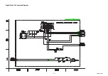
Page 37: ...8 8 A81N5SCF Function Junction Schematic Diagram ...

Page 38: ...8 9 A81N5SCIR IR Sensor Junction Schematic Diagram ...

Page 39: ...8 10 A81N5SCD1 DTV Module 1 2 Schematic Diagram ...

Page 40: ...8 11 A81N5SCD2 DTV Module 2 2 Schematic Diagram ...

Page 41: ...8 12 A81N5SCDM1 Digital Main 1 6 Schematic Diagram ...

Page 42: ... Main 2 6 Schematic Diagram The order of pins shown in this diagram is different from that of actual IC1201 IC1201 is divided into four and shown as IC1201 1 4 IC1201 4 4 in this Digital Main Schematic Diagram Section 1 NOTE ...

Page 43: ... Main 3 6 Schematic Diagram The order of pins shown in this diagram is different from that of actual IC1201 IC1201 is divided into four and shown as IC1201 1 4 IC1201 4 4 in this Digital Main Schematic Diagram Section 1 NOTE ...

Page 44: ... Main 4 6 Schematic Diagram The order of pins shown in this diagram is different from that of actual IC1201 IC1201 is divided into four and shown as IC1201 1 4 IC1201 4 4 in this Digital Main Schematic Diagram Section 1 NOTE ...

Page 45: ... Main 5 6 Schematic Diagram The order of pins shown in this diagram is different from that of actual IC1201 IC1201 is divided into four and shown as IC1201 1 4 IC1201 4 4 in this Digital Main Schematic Diagram Section 1 NOTE ...

Page 46: ...8 17 A81N5SCDM6 Digital Main 6 6 Schematic Diagram ...

Page 47: ...f fire replace only with same type 4 A 125V fuse CAUTION ATTENTION Utiliser un fusible de rechange de même type de 4A 125V 4A 125V CAUTION Fixed voltage or Auto voltage selectable power supply circuit is used in this unit If Main Fuse F601 is blown check to see that all components in the power supply circuit are not defective before you connect the AC plug to the AC power supply Otherwise it may c...

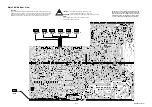
Page 48: ...lation transformer is required For continued protection against risk of fire replace only with same type 4 A 125V fuse CAUTION ATTENTION Utiliser un fusible de rechange de même type de 4A 125V 4A 125V CAUTION Fixed voltage or Auto voltage selectable power supply circuit is used in this unit If Main Fuse F601 is blown check to see that all components in the power supply circuit are not defective be...

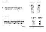
Page 49: ...8 20 Function CBA Top View Function CBA Bottom View BA81N0F01022 2 IR Sensor CBA Top View IR Sensor CBA Bottom View BA81N0F01022 5 BA81N0F01022 3 Junction CBA Top View Junction CBA Bottom View ...

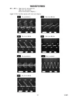
Page 50: ...aveform check points Shown in Schematic Diagram CVBS 0 2V 20µs WF1 Pin 6 of CN703 S VIDEO Y 0 2V WF2 Pin 10 of CN703 20µs S VIDEO C 0 2V WF3 Pin 8 of CN703 20µs AUDIO 0 1V 0 5ms WF7 Pin 14 of IC801 COMP Pr 0 2V 20µs Pin 14 of CN703 WF6 COMP Pb 0 2V 20µs Pin 15 of CN703 WF5 COMP Y 0 2V 20µs Pin 12 of CN703 WF4 ...

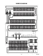
Page 51: ...TV S SCLK GND DTV ON H DTV ON H2 DTV S SREQ CN1503 CN703 1 3 2 5 4 7 6 8 9 10 13 12 11 14 15 17 16 19 18 21 20 22 23 23 21 22 19 20 17 18 16 15 14 11 12 13 10 9 7 8 5 6 3 4 2 1 GND S VIDEO Y GND S VIDEO C GND CVBS GND VOLUME AUDIO MUTE PROTECT 4 NU COMP Y GND COMP Pr COMP Pb GND DTV Pr DTV Pb GND DTV Y GND PC AUDIO L PC AUDIO R WH1101 CN705 CN706 IR SENSOR CBA 1 3 2 4 1 3 2 4 AL 3 3V D REMOTE GND ...

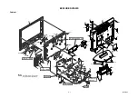
Page 52: ... L1 S5 L6 L1 L1 A7 A3 L1 SP801 SP802 See Electrical Parts List for parts with this mark Main CBA AC601 Function CBA IR Sensor CBA B11 B11 B11 B10 B2 L1 L1 L3 L2 L2 L1 L4 L4 L4 L1 L1 B6 B9 DTV Module CBA Unit B7 A12 A12 A9 LCD1 A11 L1 L3 Digital Main CBA Unit Junction CBA CLN802 CL1901 CL1902 L3 L19 CLN801 ...

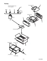
Page 53: ... 2 A81N5PEX Packing S1 FRONT S3 S6 S4 Tape Tape Packing Tape Packing Tape Packing Tape S2 X1 Some Ref Numbers are not in sequence X4 X5 L6 X3 X2 Packing Tape Stand Assembly Packing Tape S5 Packing Tape S7 ...

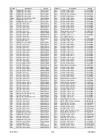
Page 54: ...EM322705 B7 ARM ASSEMBLY A72N0JH 1EM221634 B9 MODULE PCB HOLDER P7150UT 1EM322373A CL1901 WIRE ASSEMBLY FFC FFC 40PIN WX1A81N0 01A CL1902 WIRE ASSEMBLY FFC FFC 40PIN WX1A81N0 01A CLN801 WIRE ASSEMBLY SPEAKER 2PIN AWG24 WX1A81N0 05A CLN802 WIRE ASSEMBLY SPEAKER 2PIN AWG24 WX1A81N0 05A L1 SCREW P TIGHT M3X10 BIND HEAD GBJP3100 L2 SCREW P TIGHT 3X10 BIND HEAD GBHP3100 L3 SCREW S TIGHT M3X6 BIND HEAD ...

Page 55: ...47pF 50V CHD1JJ3CH470 C74 CHIP CERAMIC CAP F Z 1µF 10V CHD1AZ30F105 C75 CHIP CERAMIC CAP F Z 1µF 10V CHD1AZ30F105 C77 CHIP CERAMIC CAP 1608 F Z 0 1µF 25V CHD1EZ30F104 C80 CHIP CERAMIC CAP 1608 B K 1000pF 50V CHD1JK30B102 C83 CHIP RES 1608 1 10W 0 Ω RRXAZR5Z0000 C84 CHIP CERAMIC CAP 1608 F Z 0 1µF 25V CHD1EZ30F104 C85 CHIP CERAMIC CAP CH J 330pF 50V CHD1JJ3CH331 C86 CHIP CERAMIC CAP CH J 330pF 50V ...

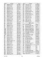
Page 56: ...0pF 50V CHD1JK30B472 C891 CHIP CERAMIC CAP 1608 B K 4700pF 50V CHD1JK30B472 C892 CHIP CERAMIC CAP F Z 1µF 10V CHD1AZ30F105 C893 CHIP CERAMIC CAP F Z 1µF 10V CHD1AZ30F105 C894 ELECTROLYTIC CAP 10µF 50V M CE1JMASDL100 Ref No Description Part No C901 ELECTROLYTIC CAP 2200µF 25V M CE1EMZNDL222 C902 ELECTROLYTIC CAP 470µF 25V M CE1EMASDL471 C903 ELECTROLYTIC CAP 1000µF 16V M CE1CMZNDL102 C904 ELECTROLY...

Page 57: ...TCHING DIODE 1SS133 T 77 QDTZ001SS133 D930 ZENER DIODE MTZJT 775 6B QDTB0MTZJ5R6 D932 DIODE FR154 NDLZ000FR154 D933 ZENER DIODE MTZJT 775 6B QDTB0MTZJ5R6 Ref No Description Part No D934 SWITCHING DIODE 1SS133 T 77 QDTZ001SS133 D940 ZENER DIODE MTZJT 7710B QDTB00MTZJ10 D942 SWITCHING DIODE 1SS133 T 77 QDTZ001SS133 D947 PCB JUMPER D0 6 P5 0 JW5 0T D948 PCB JUMPER D0 6 P5 0 JW5 0T D951 SWITCHING DIOD...

Page 58: ... RES 1 4W J 100 Ω RCX4JATZ0101 R410 CHIP RES 1 10W J 10k Ω RRXAJR5Z0103 Ref No Description Part No R411 CHIP RES 1 10W J 3 3k Ω RRXAJR5Z0332 R412 CARBON RES 1 4W J 10k Ω RCX4JATZ0103 R413 CARBON RES 1 4W J 1 2k Ω RCX4JATZ0122 R414 CHIP RES 1 10W J 47 Ω RRXAJR5Z0470 R415 CHIP RES 1 10W J 10k Ω RRXAJR5Z0103 R416 CARBON RES 1 4W J 470 Ω RCX4JATZ0471 R417 CARBON RES 1 4W J 5 6k Ω RCX4JATZ0562 R418 CHI...

Page 59: ... RES 1 10W J 100k Ω RRXAJR5Z0104 R823 CHIP RES 1 10W J 100k Ω RRXAJR5Z0104 Ref No Description Part No R824 CHIP RES 1 10W J 100k Ω RRXAJR5Z0104 R825 CHIP RES 1 10W J 100k Ω RRXAJR5Z0104 R826 CARBON RES 1 4W J 100k Ω RCX4JATZ0104 R827 CHIP RES 1 10W J 100k Ω RRXAJR5Z0104 R828 CHIP RES 1 10W J 100k Ω RRXAJR5Z0104 R829 CHIP RES 1 10W J 100k Ω RRXAJR5Z0104 R830 CHIP RES 1 10W J 100k Ω RRXAJR5Z0104 R83...

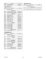
Page 60: ...ES 1 4W J 100 Ω RCX4JATZ0101 R1005 CHIP RES 1 10W F 4 7k Ω RRXAFR5H4701 Ref No Description Part No R1006 CHIP RES 1 10W F 4 7k Ω RRXAFR5H4701 R1007 CHIP RES 1 10W F 2 2k Ω RRXAFR5H2201 R1008 CHIP RES 1608 1 10W 0 Ω RRXAZR5Z0000 R1010 CARBON RES 1 4W J 47k Ω RCX4JATZ0473 R1011 CARBON RES 1 4W J 22k Ω RCX4JATZ0223 R1012 CHIP RES 1 10W J 10k Ω RRXAJR5Z0103 R1013 CHIP RES 1 10W J 3 3k Ω RRXAJR5Z0332 R...

Page 61: ...ITCH SKQSAB SST0101AL038 SW1104 TACT SWITCH SKQSAB SST0101AL038 SW1105 TACT SWITCH SKQSAB SST0101AL038 SW1106 TACT SWITCH SKQSAB SST0101AL038 SW1107 TACT SWITCH SKQSAB SST0101AL038 SW1113 TACT SWITCH SKQSAB SST0101AL038 MISCELLANEOUS BC1101 PCB JUMPER D0 6 P5 0 JW5 0T Ref No Description Part No IR SENSOR CBA Consists of the following CAPACITOR C1151 CHIP CERAMIC CAP F Z 1µF 10V CHD1AZ30F105 DIODES...

Page 62: ...erein without the obligation to notify any person or organization of such changes with the design is a registered trademark of Funai Electric Co Ltd and may not be used in any way without the express written consent of Funai All other trademarks used herein remain the exclusive property of their respective owners Nothing contained in this manual should be construed as granting by implication or ot...

Reviews: