Functional Description
RTM-ATCA-F140 Installation and Use (6806800M97A)
55
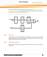
The conversion process depends on which input frequency is in use.
shows the process. A register setting for each of the two reference
outputs selects between the two input frequencies.
4.8.8
SPI Flash
The SPI ports from the BCM8727, BCM84754, and BCM84740 connect to the FPGA along with
three SPI Flash devices, one for each type. Register settings allow access to be granted to any of
the PHYs and also provide a programming port.
4.8.9
FPGA Register Map
Details of the FPGA register map are included in the RTM FPGA section of the ATCA-F140 FPGA
design guide.
Figure 4-6
Synchronous Ethernet Reference Recovery
Digital
Frequency
Synthesizer
x32
Synchronous
Divider
/25
Synchronous
Divider
/25782 ,
25781 , 25781 ,
25781
(25781 .25
overall)
161.1328125 MHz
8 kHz
Synchronous
Divider
/19532 ,
19531 , 19531 ,
19531
(19531 .25
overall)
156.25 MHz
EA Version
Summary of Contents for RTM-ATCA-F140
Page 6: ...RTM ATCA F140 Installation and Use 6806800M97A Contents 6 Contents Contents EA Version ...
Page 8: ...RTM ATCA F140 Installation and Use 6806800M97A 8 List of Tables EA Version ...
Page 10: ...RTM ATCA F140 Installation and Use 6806800M97A 10 List of Figures EA Version ...
Page 20: ...Introduction RTM ATCA F140 Installation and Use 6806800M97A 20 EA Version ...
Page 34: ...Controls LEDs and Connectors RTM ATCA F140 Installation and Use 6806800M97A 34 EA Version ...
Page 58: ...Functional Description RTM ATCA F140 Installation and Use 6806800M97A 58 EA Version ...
Page 60: ...Related Documentation RTM ATCA F140 Installation and Use 6806800M97A 60 EA Version ...
Page 70: ...Index RTM ATCA F140 Installation and Use 6806800M97A 70 EA Version ...
Page 71: ...EA Version ...

