background image


Safety Notes

CPCI-6200 Installation and Use (6806800J66C)

187

Operation

 Product 

Damage

High humidity and condensation on surfaces cause short circuits. 
Do not operate the product outside the specified environmental limits. Make sure the product 
is completely dry and there is no moisture on any surface before applying power.


Personal Injury or Death
This product operates with dangerous voltages that can cause injury or death. 
Use extreme caution when handling, testing, and adjusting this equipment and its 
components. 

Battery

 Data 

Loss

Installing another battery type than the one that is mounted at product delivery may cause 
data loss since other battery types may be specified for other environments or may have a 
shorter lifetime. 
Only use the same type of lithium battery as is already installed.


PCB and Battery Holder Damage
Removing the battery with a screw driver may damage the PCB or the battery holder. 
Do not use a screw driver to remove the battery from its holder.

 Product 

Damage

Incorrect replacement of lithium batteries can result in a hazardous explosion.
When exchanging the on-board lithium battery, make sure that the new and the old battery 
are exactly the same battery models.
If the respective battery model is not available, contact your local Emerson sales 
representative for the availability of alternative officially approved battery models.   

Summary of Contents for CPCI-6200

Page 1: ...Embedded Computing for Business Critical ContinuityTM CPCI 6200 Installation and Use P N 6806800J66C August 2011 ...

Page 2: ...document and to make changes from time to time in the content hereof without obligation of Emerson to notify any person of such revision or changes Electronic versions of this material may be read online downloaded for personal use or referenced in another document as a URL to a Emerson website The text itself may not be published commercially in print or electronic form edited translated or other...

Page 3: ...31 2 5 Installing Accessories 32 2 5 1 Installing a PMC Module on the CPCI Baseboard 32 2 5 2 Installing the Rear Transition Module 34 2 6 Preparing the Baseboard for Installation 34 2 6 1 Inspecting the CPCI Baseboard 34 2 6 2 Equipment Required for Installation 35 2 6 3 Hardware Configuration 35 2 6 3 1 Board Configuration Switch S1 36 2 6 3 2 IPMI Configuration Switch S2 38 2 7 Installing the C...

Page 4: ...XJ1 and XJ2 60 3 3 12 PCI Express Expansion Connector J17 62 3 3 13 IPMI Debug and FW Programming Header P3 64 3 3 14 Processor Debug Header P4 64 3 3 15 Boundary Scan Header P5 65 3 3 16 Processor COP Header P6 65 3 3 17 PCI Express Switch Header P7 66 3 4 Switches 66 3 4 1 Onboard Switches 66 3 4 2 Reset Abort Switch P2 67 3 5 Front Panel LEDs 67 3 6 Status Indicators 68 4 Functional Description...

Page 5: ...3 USB PCI Bus 4 81 4 10 4 PCI Bus Frequency 81 4 11 Operation Modes 81 4 11 1 System Controller Mode 82 4 11 2 Peripheral Mode 82 4 11 3 Stand Alone Mode 83 4 12 PCI Express Expansion 84 4 13 System Interrupts 85 4 14 Clock Distribution 86 4 15 MPC8572 System Clock 87 4 16 Reset Control Logic 87 4 16 1 Abort Reset Switch 89 4 16 2 Reset Timing 90 4 17 RTC Battery 91 4 18 IPMI Controller 91 4 18 1 ...

Page 6: ...mmands 107 6 1 1 Global IPMI Commands 107 6 1 2 Watchdog Commands 107 6 1 3 IPMI Messaging Commands 108 6 1 4 SEL Device Commands 108 6 1 5 SDR Repository Commands 109 6 1 6 FRU Inventory Commands 109 6 1 7 Sensor Device Commands 110 6 1 8 Chassis Device Commands 111 6 2 PICMG 2 9 Commands 111 6 3 Emerson Specific Commands 112 6 3 1 Firmware Upgrade Commands 112 6 3 1 1 Start Firmware Upgrade 113 ...

Page 7: ...ct Register 154 7 4 11 NAND Flash Chip 1 Presence Register 155 7 4 12 NAND Flash Chip 1 Status Register 156 7 4 13 NAND Flash Chip 2 Control Register 157 7 4 14 NAND Flash Chip 2 Select Register 158 7 4 15 NAND Flash Chip 2 Presence Register 159 7 4 16 NAND Flash Chip 2 Status Register 160 7 4 17 CPCI Control and Status Register 161 7 4 18 Geographic Address Read Register 162 7 4 19 Watchdog Timer...

Page 8: ...PCI IDSEL and Interrupt Assignment 176 7 7 2 PCI Vendor and Device IDs 176 7 7 3 PCI Arbitration Assignments 177 A Replacing the Battery 179 A 1 Battery Location 179 A 2 Replacing the Battery 180 B Related Documentation 181 B 1 Emerson Network Power Embedded Computing Documents 181 B 2 Manufacturer s Publications 182 B 3 Related Specifications 183 Safety Notes 185 Sicherheitshinweise 189 Index 193...

Page 9: ...55 Table 3 9 PMC Connector Pin Assignments J14 J24 56 Table 3 10 Front Panel Latch Pinout P1 59 Table 3 11 DDR3 SO DIMMs Pinout XJ1 and XJ2 60 Table 3 12 PCI Express Expansion Connector Pinout J17 62 Table 3 13 IPMI Debug Pinout P3 64 Table 3 14 Processor Debug Header Pinout P4 64 Table 3 15 Boundary Scan Header Pinout P5 65 Table 3 16 COP Header Pinout P6 65 Table 3 17 PCI Express Switch Header P...

Page 10: ...ble 6 16 OEM Commands 115 Table 6 17 Request Data of BMC PM Change Role 116 Table 6 18 Response Data of BMC PM Change Role 116 Table 6 19 Request Data of Get Geographical Address 117 Table 6 20 Response Data of Get Geographical Address 117 Table 6 21 FRU Information CPCI 6200 118 Table 6 22 IPMI Sensors Overview 118 Table 6 23 Aggregate T Sensor 120 Table 6 24 Aggregate V Sensor 121 Table 6 25 CPC...

Page 11: ...9 Table 7 17 Interrupt Mask Register 0xF200_0006 150 Table 7 18 Interrupt Mask Register 150 Table 7 19 Presence Detect Register 0xF200_0008 151 Table 7 20 Presence Detect Register Field Definition 152 Table 7 21 NAND Flash Chip 1 Control Register 0xF200_0010 153 Table 7 22 NAND Flash Chip 1 Control Register Field Definition 153 Table 7 23 NAND Flash Chip 1 Select Register 0xF200_0011 154 Table 7 2...

Page 12: ...ter Register 0xF200_0026 166 Table 7 47 PLD Revision Register 0xF200_0030 167 Table 7 48 PLD Revision Register Field Definition 167 Table 7 49 PLD Date Code Register 0xF200_0034 168 Table 7 50 PLD Date Code Register Field Definition 168 Table 7 51 Test Register 1 0xF200_0038 168 Table 7 52 Test Register 2 0xF200_003C 169 Table 7 53 Prescaler Register 0xE202_0000 169 Table 7 54 Tick Timer Control R...

Page 13: ...8 Figure 3 3 Serial Port Connector Pinout J16 59 Figure 4 1 CPCI 6200 Block Diagram 72 Figure 4 2 Boot Block A 76 Figure 4 3 Boot Block B 77 Figure 4 4 PCI Express Bus Topology 79 Figure 4 5 System Controller Mode 82 Figure 4 6 Peripheral Mode 83 Figure 4 7 Stand Alone Mode 84 Figure 4 8 Routing of Interrupt Sources 85 Figure 4 9 CPCI 6200 Clock Distribution Diagram 86 Figure 7 1 CPCI 6200 Memory ...

Page 14: ...CPCI 6200 Installation and Use 6806800J66C 14 List of Figures ...

Page 15: ...vides an overview and description of basic MOTLoad use including implementation issues a list of the initialization sequence and a description of basic commands Control via IPMI discusses the IPMI commands that the product supports Memory Maps and Addresses provides details on the various registers and addresses used in the product Replacing the Battery provides instructions on how to replace the ...

Page 16: ...asable Programmable Read Only Memory ESD Electrostatic Sensitive Device ETSI European Telecommunication Standards Institute FCC Federal Communications Commission FRU Field Replaceable Unit GMII Gigabit Media Independent Interface GPCM General Purpose Chip select Machine IEEE Institute of Electrical and Electronics Engineers IPMB Intelligent Platform Management Bus IPMC Intelligent Platform Managem...

Page 17: ...Interrupt Controller PIM PCI Mezzanine Card Input Output Module PICMG PCI Industrial Computer Manufacturers Group PMC PCI Mezzanine Card PM Peripheral Management PLD Programmable Logic Device PLL Phase Locked Loop PrPMC Processor PCI Mezzanine Card Rcv Receive RTC Real Time Clock RTM Rear Transition Module SBC Single Board Computer SDR Sensor Data Record SDRAM Synchronous Dynamic Random Access Mem...

Page 18: ...x00000000 Typical notation for hexadecimal numbers digits are 0 through F for example used for addresses and offsets 0b0000 Same for binary numbers digits are 0 and 1 bold Used to emphasize a word Screen Usedforon screenoutputandcoderelatedelements or commands in body text Courier Bold Used to characterize user input and to separate it from system output Reference Used for references and for table...

Page 19: ...R Indicates a hazardous situation which if not avoided could result in death or serious injury Indicates a hazardous situation which if not avoided may result in minor or moderate injury Indicates a property damage message No danger encountered Pay attention to important information Notation Description Part Number Publication Date Description 6806800J66C August 2011 Updated Appendix P Safety Note...

Page 20: ...CPCI 6200 Installation and Use 6806800J66C About this Manual 20 About this Manual ...

Page 21: ...s interfaces 8 lanes of 2 5 Gb s each Four integrated 10 100 1000 Ethernet controllers One integrated DUART Two integrated I2 C controllers One integrated programmable interrupt controller One integrated local bus controller System Memory Two banks of DDR3 SDRAM with error correcting code ECC Supports 2 or 4 GB Provides up to 800 MHz DDR3 data rate I2 C One 8 KB VPD serial EEPROM Two 64 KB user co...

Page 22: ...I O Timers Eight 32 bit MCP8572 timers Four 32 bit timers in a PLD One watchdog timer in PLD CPCI Interface Complies with the following PCI Specification Revision 2 2 PICMG 2 1 R2 0 CompactPCI Hot Swap Specification January 17 2001 PICMG 2 0R3 0CompactPCICore Specification October 1 1999 PICMG 2 16 R1 0 CompactPCI Packet Switching Backplane Specification September 5 2001 PICMG 2 9 R1 0 CompactPCI ...

Page 23: ...tch on the face plate User Fail LED on the face plate Blue hot swap LED on the face plate One standard 16 pin JTAG COP header Support for boundary scan Software Support VxWorks Linux RTM Compatible with RTM CPCI 6115 01 W3766F11A Table 1 1 Summary of Features continued Function Features ...

Page 24: ... 60950 1 Safety Requirements legal CISPR 22 CISPR 24 EN 55022 EN 55024 FCC Part 15 Industry Canada ICES 003 VCCI Japan AS NZS CISPR 22 EN 300 386 NEBS Standard GR 1089 CORE EMC requirements legal on system level predefined Emerson system NEBS Standard GR 63 CORE ETSI EN 300 019 series Environmental Requirements Directive 2002 95 EC Directive on the restriction of the use of certain hazardous subst...

Page 25: ...Introduction CPCI 6200 Installation and Use 6806800J66C 25 Figure 1 1 Declaration of Conformity ...

Page 26: ...owing sections when ordering boards and accessories 1 4 1 Supported Board Models 1 4 2 Board Accessories Table 1 2 Order Numbers for Baseboard Variants Marketing Number Description CPCI6200 13 2G MPC8572 1 33 GHz 2 GB SO DIMM DDR3 6E CPCI6200 15 4G MPC8572 1 5 GHz 4 GB SO DIMM DDR3 6E Table 1 3 Order Numbers for Related Products Marketing Number Description CPCI 6115 MCPTM 02 Transition module PIM...

Page 27: ...Introduction CPCI 6200 Installation and Use 6806800J66C 27 1 5 Product Identification Figure 1 2 Location of the Product Serial Number 9105991 Serial Number Label ...

Page 28: ...Introduction CPCI 6200 Installation and Use 6806800J66C 28 ...

Page 29: ...acking the CPCI Baseboard 1 Make sure that you receive all items of your shipment Printed Quick Start Guide and Safety Notes CPCI 6200 baseboard Optional items that were ordered 2 Check the board for damages and report any damage to Emerson 3 Remove the desiccant bag shipped together with the board and dispose of it according to your country s legislation The product is thoroughly inspected before...

Page 30: ...ntal requirements must also be taken into account Product Damage High humidity and condensation on surfaces cause short circuits Do not operate the product outside the specified environmental limits Make sure the product is completely dry and there is no moisture on any surface before applying power Table 2 1 CPCI 6200 Environmental Requirements Characteristics Operating Non Operating Operating Te...

Page 31: ... using For information on the accessories power requirements refer to the documentation delivered with the respective accessory or ask your local representative Shock Half sine 11 ms 30 ms Blade level packaging Half sine 6 ms at 180 ms Free Fall Blade level packaging 100 mm unpackaged per GR 63 CORE Table 2 1 CPCI 6200 Environmental Requirements continued Characteristics Operating Non Operating Ta...

Page 32: ...ap must be secured to your wrist and to ground throughout the procedure 2 Remove chassis or system cover s as necessary for access to the board 3 Carefully remove the CPCI 6200 from the card slot and lay it flat with connectors J1 through J5 facing you Damage of Circuits Electrostatic discharge and incorrect installation and removal of the product can damage circuits or shorten their life Before t...

Page 33: ...PCI 6200 5 Make sure that hole on the PMC matches the voltage key on CPCI 6200 Do not remove the PMC voltage key 6 Slide the edge connector of the PMC module into the front panel opening from behind and then place the PMC module on top of the baseboard PMC Filler Plate PMC Alignment Voltage Key CPCI 6200 supports only 3 3 V I O PMC modules ...

Page 34: ...d Installation chapter in the CPCI 6115 CompactPCI Single Board Computer Installation and Use manual 2 6 Preparing the Baseboard for Installation 2 6 1 Inspecting the CPCI Baseboard You can use the CPCI 6200 as a system controller in a system slot an intelligent I O board in a peripheral slot or in stand alone mode The board is fully compliant to CompactPCI Hot Swap Specification PICMG 2 1 R2 0 an...

Page 35: ... 6 2 Equipment Required for Installation You need the following items to do a complete installation CompactPCI or compatible system enclosure System console terminal Operating system and or application software Disk drives or other I O and controllers 2 6 3 Hardware Configuration To produce the desired configuration and ensure proper operation of the board you may need to carry out certain hardwar...

Page 36: ...chsettingsare described in the succeeding sections 2 6 3 1 Board Configuration Switch S1 The CPCI 6200 uses an 8 position SMT configuration switch to Control the flash bank write protect Select the flash boot image Control the safe start ENV settings Figure 2 1 Location of Configuration Switches Board Configuration Switch S1 IPMI Configuration Switch S2 ...

Page 37: ...e PMC1_PCI_FSEL switch is OFF the maximum PCI bus operation is 100 MHz on PMC1 When it is ON the maximum PCI bus operation is 100 MHz on PMC1 For more information see PCI Bus Frequency on page 81 Table 2 3 S1 Switch Settings Switch Name ON OFF Default SW1 SAFE_START Use safe ENV setting Use normal ENV setting SW2 BOOT_SEL Boardisbootedfromblock B of Flash A Board is booted from block A of Flash A ...

Page 38: ...hen a 12 V supply is not available in the system or chassis 2 6 3 2 IPMI Configuration Switch S2 The CPCI 6200 uses an 8 position SMT configuration switch to control the IPMI controller settings The default switch position is OFF When the IPMI_DISABLE switch is OFF the IPMI device is enabled When the switch ON IPMI is disabled by asserting its reset Table 2 4 S2 Switch Settings Switch Name ON OFF ...

Page 39: ...maximum 100 MHz PCI bus frequency can be used on PMC2 When the switch is ON the maximum PCI bus frequency is 133 MHz For more information see PCI Bus Frequency on page 81 2 7 Installing the CPCI Baseboard 1 Attach an ESD strap to your wrist and then attach the other end of the ESD strap to the chassis as a ground The ESD strap must be secured to your wrist and to ground throughout the procedure 2 ...

Page 40: ... emissions 9 Replace the chassis or system cover s and make sure no cables are pinched 10 Cable the peripherals to the panel connectors and then reconnect the system to the AC or DC power source 11 Turn the equipment power on After you have verified that all necessary hardware preparation has been done that all connections have been made correctly and that the installation is complete you can powe...

Page 41: ...ess the red button to unlock handles 3 Open handles until resistance is encountered The hot swap switch opens automatically Data Loss Removing the RTM with the system power on and the blue LED on the front blade still flashing causes data loss Before removing the RTM from a powered system power down the slot and the front blade s payload by opening the lower handle of the front blade and wait unti...

Page 42: ...ity Baud rate of 9600 9600 baud is the power up default for serial ports on CPCI 6200 boards After power up you can reconfigure the baud rate if you wish using the MOTLoad PF Port Format command via the command line interface Whatever the baud rate some type of hardware handshaking either XON OFF or via the RTS CTS line is desirable if the system supports it 2 10 Factory Installed Linux A bootable...

Page 43: ...lowing prompt Emerson Network Power Embedded Computing Linux Kernel 2 6 29 6 on a 2 processor CPCI6200 localhost login Login as root with no password If you want to use IPMI load the IPMI SMBus driver using modprobe ipmi_smb Contact Emerson for kernel patches and additional information on using Linux on the CPCI 6200 ...

Page 44: ...Hardware Preparation and Installation CPCI 6200 Installation and Use 6806800J66C 44 ...

Page 45: ...oard Layout J5 J3 J2 J1 NAND Flash DDR3 DIMM COP Header Processor Configuration Switch S1 Configuration Switch S2 PCI Express Expansion Connector USB Controller JTAG Header IPMI Controller RTC Battery Boot Flash PCI Express x4 to PCI Bridge 1 2 3 PCI Express Switch PMC 2 PMC 1 PCI x1 to PCI Bridge DDR3 DIMM LBC PLD ...

Page 46: ...or more information on the front panel connectors see Front Panel LEDs on page 67 Cutout for PMC Slot 2 covered with filler panel Cutout for PMC Slot 1 covered with filler panel Ethernet Port 1 Ethernet Port 2 Reset Abort Switch Hot Swap LED Blue User Fail LED Green Yellow USB Port Serial Port ...

Page 47: ...Ethernet Ethernet port on the front panel ENET 1 and ENET2 J7 USB port on the front panel J11 J12 J13 J14 PMC1 J21 J22 J23 J24 PMC2 J16 Serial Port 1 COM1 Mini DB9 serial port on the front panel J17 PMC expansion to PMCspan P1 Board insertion ejection Switch connector on the front panel P2 Reset abort switch on the front panel P3 IPMI serial port COM2 Planar header for debugging IPMI Serial Port P...

Page 48: ...functionality Table 3 1 Onboard Connectors continued Reference Designator Function Table 3 2 CPCI Bus Connector Pinout J1 Pin Row A Row B Row C Row D Row E 25 5 0 V REQ64 ENUM 3 3 V 5 0 V 24 AD 1 5 0 V V IO 1 AD 0 ACK64 23 3 3 V AD 4 AD 3 5 0 V1 AD 2 22 AD 7 GND 3 3 V1 AD 6 AD 5 21 3 3 V AD 9 AD 8 M66EN C BE 0 20 AD 12 GND V IO AD 11 AD 10 19 3 3 V AD 15 AD 14 GND1 AD 13 18 SERR GND 3 3 V PAR C BE...

Page 49: ... 5 0 V TMS TDO TDI 1 5 0 V 12 V TRST 12 V 5 0 V Table 3 2 CPCI Bus Connector Pinout J1 continued Pin Row A Row B Row C Row D Row E Table 3 3 CPCI Bus Connector Pinout J2 Pin Row A Row B Row C Row D Row E 22 GA4 GA3 GA2 GA1 GA0 21 RSV GND RSV RSV RSV 20 RSV GND RSV GND RSV 19 GND GND RSV RSV RSV 18 BRSVP2A18 BRSVP2B18 BRSVP2C18 GND BRSVP2E18 17 BRSVP2A17 GND RSV RSV RSV 16 BRSVP2A16 BRSVP2B16 RSV G...

Page 50: ...V RSV SYSEN 1 RSV RSV 1 RSV GND RSV RSV RSV 1 Defined as SYSEN This OV allows the CPCI 6200 to ensure that it is installed into a peripheral slot Table 3 3 CPCI Bus Connector Pinout J2 continued Pin Row A Row B Row C Row D Row E Table 3 4 CPCI User I O Connector Pinout J3 Pin Row A Row B Row C Row D Row E 1 IPMI_PWR PMCIO64 PMCIO63 PMCIO62 PMCIO61 2 PMCIO60 PMCIO59 PMCIO58 PMCIO57 PMCIO56 3 PMCIO5...

Page 51: ...lated 3 3 5 CPCI User I O Connector J5 J5 is a five row user I O CPCI connector 9 PMCIO25 PMCIO24 PMCIO23 PMCIO22 PMCIO21 10 PMCIO20 PMCIO19 PMCIO18 PMCIO17 PMCIO16 11 PMCIO15 PMCIO14 PMCIO13 PMCIO12 PMCIO11 12 PMCIO10 PMCIO9 PMCIO8 PMCIO7 PMCIO6 13 PMCIO5 PMCIO4 PMCIO3 PMCIO2 PMCIO1 14 3 3V 3 3V 3 3V 5V 5V 15 G1_DB RX2 G1_DB RX2 GND G1_DD G1_DD 16 G1_DA TX2 G1_DA TX2 GND G1_DC G1_DC 17 G0_DB RX1 ...

Page 52: ...O51 4 PMCIO50 PMCIO49 PMCIO48 PMCIO47 PMCIO46 5 PMCIO45 PMCIO44 PMCIO43 PMCIO42 PMCIO41 6 PMCIO40 PMCIO39 PMCIO38 PMCIO37 PMCIO36 7 PMCIO35 PMCIO34 PMCIO33 PMCIO32 PMCIO31 8 PMCIO30 PMCIO29 PMCIO28 PMCIO27 PMCIO26 9 PMCIO25 PMCIO24 PMCIO23 PMCIO22 PMCIO21 10 PMCIO20 PMCIO19 PMCIO18 PMCIO17 PMCIO16 11 PMCIO15 PMCIO14 PMCIO13 PMCIO12 PMCIO11 12 PMCIO10 PMCIO9 PMCIO8 PMCIO7 PMCIO6 13 PMCIO5 PMCIO4 PM...

Page 53: ...J21 Pin 1 TCK 12 V 2 3 GND INTA 4 5 INTB INTC 6 7 PRESENT 5 V 8 9 INTD PCI_RSVD 10 11 GND NC 3 3Vaux 12 13 CLK GND 14 15 GND GNT XREQ0 16 17 REQ XGNT0 5 V 18 19 VIO AD31 20 21 AD28 AD27 22 23 AD25 GND 24 25 GND C BE3 26 27 AD22 AD21 28 29 AD19 5 V 30 31 VIO AD17 32 33 FRAME GND 34 35 GND IRDY 36 37 DEVSEL 5 V 38 39 PCIXCAP LOCK 40 41 PCI_RSVD PCI_RSVD 42 43 PAR GND 44 45 VIO AD15 46 47 AD12 AD11 4...

Page 54: ...PMC Connector Pinout J12 J22 Pin J12 J22 Pin 1 12 V TRST 2 3 TMS TDO 4 5 TDI GND 6 7 GND PCI_RSVD 8 9 PCI_RSVD PCI_RSVD 10 11 MOT_RSVD 3 3 V 12 13 RST MOT_RSVD 14 15 3 3 V MOT_RSVD 16 17 NC PME GND 18 19 AD30 AD29 20 21 GND AD26 22 23 AD24 3 3 V 24 25 IDSEL AD23 26 27 3 3 V AD20 28 29 AD18 GND 30 31 AD16 C BE2 32 33 GND IDSELB 34 Table 3 6 PMC Connector Pinout J11 J21 continued Pin J11 J21 Pin ...

Page 55: ... 51 AD07 REQB_L 52 53 3 3 V GNTB_L 54 55 MOT_RSVD GND 56 57 MOT_RSVD EREADY 58 59 GND NC RESETOUT_L 60 61 ACK64 3 3 V 62 63 GND NC MONARCH 64 Table 3 8 PMC Connector Pinout J13 J23 Pin J13 J23 Pin 1 PCI_RSVD GND 2 3 GND C BE7 4 5 C BE6 C BE5 6 7 C BE4 Note 1 GND 8 9 VIO PAR64 10 11 AD63 AD62 12 13 AD61 GND 14 15 GND AD60 16 17 AD59 AD58 18 Table 3 7 PMC Connector Pinout J12 J22 continued Pin J12 J...

Page 56: ...34 35 AD47 AD46 36 37 AD45 GND 38 39 VIO AD44 40 41 AD43 AD42 42 43 AD41 GND 44 45 GND AD40 46 47 AD39 AD38 48 49 AD37 GND 50 51 GND AD36 52 53 AD35 AD34 54 55 AD33 GND 56 57 VIO AD32 58 59 PCI_RSVD PCI_RSVD 60 61 PCI_RSVD GND 62 63 GND PCI_RSVD 64 Table 3 9 PMC Connector Pin Assignments J14 J24 Pin J14 J24 Pin 1 PMCIO1 PMCIO2 2 Table 3 8 PMC Connector Pinout J13 J23 continued Pin J13 J23 Pin ...

Page 57: ...MCIO21 PMCIO22 22 23 PMCIO23 PMCIO24 24 25 PMCIO25 PMCIO26 26 27 PMCIO27 PMCIO28 28 29 PMCIO29 PMCIO30 30 31 PMCIO31 PMCIO32 32 33 PMCIO33 PMCIO34 34 35 PMCIO35 PMCIO36 36 37 PMCIO37 PMCIO38 38 39 PMCIO39 PMCIO40 40 41 PMCIO41 PMCIO42 42 43 PMCIO43 PMCIO44 44 45 PMCIO45 PMCIO46 46 47 PMCIO47 PMCIO48 48 49 PMCIO49 PMCIO50 50 51 PMCIO51 PMCIO52 52 53 PMCIO53 PMCIO54 54 55 PMCIO55 PMCIO56 56 Table 3 ...

Page 58: ... with two RJ 45 ports The pin configuration is based on IEEE standards 802 3ab 1999 3 3 8 USB Connector There is one standard 4 pin USB connector located on the front panel 57 PMCIO57 PMCIO58 58 59 PMCIO59 PMCIO60 60 61 PMCIO61 PMCIO62 62 63 PMCIO63 PMCIO64 64 Table 3 9 PMC Connector Pin Assignments J14 J24 continued Pin J14 J24 Pin Figure 3 2 USB Connector Pinout 1 2 3 1 4 5V USB_DATA USB_DATA GN...

Page 59: ...r extraction event The latch connector on the front panel is connected to this connector Pins 1 and 2 indicate board insertion or extraction status Pin 2 is used with the PCI Bridge while pin 3 is used with the IPMI controller A closed latch indicates board insertion In this case pin 2 and 3 are shorted and FP_EJECTSW 1 BOARD_EJECT 0 Figure 3 3 Serial Port Connector Pinout J16 6 7 8 9 1 6 5 9 1 2 ...

Page 60: ...110 VDD 9 VSS 10 DQS0 111 CK0 112 PAR_IN CK1 11 DM0 12 DQS0 113 CK0 114 ERR_OUT CK1 13 DQ2 14 VSS 115 VDD 116 VDD 15 DQ3 16 DQ6 117 A10 AP 118 CS3 17 VSS 18 DQ7 119 BA0 120 CS2 19 DQ8 20 VSS 121 WE 122 RAS 21 DQ9 22 DQ12 123 VDD 124 VDD 23 VSS 24 DQ13 125 CAS 126 ODT0 25 DQS1 26 VSS 127 CS0 128 ODT1 27 DQS1 28 DM1 129 CS1 130 A13 29 VSS 30 RESET 131 VDD 132 VDD 31 DQ10 32 VSS 133 DQ32 134 DQ36 33 ...

Page 61: ... 69 CB0 70 VSS 171 DQS6 172 DM6 71 CB1 72 CB4 173 DQS6 174 DQ54 73 VSS 74 CB5 175 VSS 176 DQ55 75 DQS8 76 DM8 177 DQ50 178 VSS 77 DQS8 78 VSS 179 DQ51 180 DQ60 79 VSS 80 CB6 181 VSS 182 DQ61 81 CB2 82 CB7 183 DQ56 184 VSS 83 CB3 84 VREFCA 185 DQ57 186 DQS7 85 VDD 86 VDD 187 VSS 188 DQS7 87 CKE0 88 A15 189 DM7 190 VSS 89 CKE1 90 A14 191 DQ58 192 DQ62 91 BA2 92 A9 193 DQ59 194 DQ63 93 VDD 94 VDD 195...

Page 62: ...XJ2 continued Pin Number Signal Pin Number Signal Pin Number Signal Pin Number Signal Table 3 12 PCI Express Expansion Connector Pinout J17 Pin Number Signal Pin Number Signal 1 GND 2 GND 3 TX0_P 4 RX0_P 5 TX0_N 6 RX0_N 7 GND 8 GND 9 TX1_P 10 RX1_P 11 TX1_N 12 RX1_N 13 GND 14 GND 15 TX2_P 16 RX2_P 17 TX2_N 18 RX2_N 19 GND 20 GND 21 TX3_P 22 RX3_P 23 TX3_N 24 RX3_N 25 GND 26 GND 27 CLK_P 28 NC 29 C...

Page 63: ...GND 52 GND 53 NC 54 NC 55 NC 56 NC 57 GND 58 GND 59 NC 60 NC 61 NC 62 NC 63 GND 64 GND 65 NC 66 NC 67 NC 68 NC 69 TDI 70 TDO 71 TRST 72 I2C_CLK 73 TMS 74 I2C_DATA 75 TCK 76 PRESENT G1 GND G2 GND G3 GND G4 GND G5 GND G6 GND G7 GND G8 GND G9 GND G10 GND Table 3 12 PCI Express Expansion Connector Pinout J17 Pin Number Signal Pin Number Signal ...

Page 64: ...ing and programming IPMI firmware 3 3 14 Processor Debug Header P4 The CPCI 6200 has a 10 pin header for debugging This header can debug a DDR or LBC interface Table 3 13 IPMI Debug Pinout P3 Pin Number Signal 1 TXD 2 GND 3 RXD 4 GND Table 3 14 Processor Debug Header Pinout P4 Pin Number Signal Signal Pin Number 1 GND MCRCID_0 2 3 TRIG_IN MCRCID_1 4 5 TRIG_OUT MCRCID_2 6 7 MDVAL MCRCID_3 8 9 3 3V ...

Page 65: ...pin header to provide access to the COP function Table 3 15 Boundary Scan Header Pinout P5 Pin Number Signal Signal Pin Number 1 TCK GND 2 3 TDO GND 4 5 TMS GND 6 7 TRST GND 8 9 TDI BSCAN_EN 10 11 Key no pin NC 12 13 GND BSCAN_AW 14 15 GND NC 16 17 GND NC 18 19 GND NC 20 Table 3 16 COP Header Pinout P6 Pin Number Signal Signal Pin Number 1 CPU_TDO Not Connected 2 3 CPU_TDI CPU_TRST 4 5 Pull up CPU...

Page 66: ...cts to the Aardvark I2C SPI Host Adapter This header is only used for prototype debugging and is not installed in the released product 3 4 Switches 3 4 1 Onboard Switches For information on switch settings see Hardware Configuration on page 35 15 CPU_CKSTPO GND 16 Table 3 16 COP Header Pinout P6 continued Pin Number Signal Signal Pin Number Table 3 17 PCI Express Switch Header Pinout P7 Pin Number...

Page 67: ...ee logical LEDs on the front panel The blue LED indicates hot swap status and is used during board insertion and extraction The second LED is a bi color LED green and yellow The green LED is completely controlled by the user through the programmable register Front Panel LEDs Control and Status Register The yellow LED indicates failure The yellow LED lights up when any one or more of the following ...

Page 68: ...Green This LED is completely user programmable TSEC1 Link Speed Front panel ENET 1 SPEED Off No link Yellow 10 100 BASE T operation Green 1000 BASE T operation TSEC1 Activity Front panel ENET 1 ACT Off No activity Blinking Green Activity is proportional to bandwidth utilization TSEC2 Link Speed Front panel ENET 2 SPEED Off No link Yellow 10 100 BASE T operation Green 1000 BASE T operation TSEC2 Ac...

Page 69: ...board Yellow D30 Green D29 Off No link Yellow 10 100 BASE T operation Green 1000 BASE T operation TSEC4 Activity Onboard D27 Off No activity Blinking Green Activity is proportional to bandwidth utilization Table 3 19 CPCI 6200 Status Indicators continued Function Location Label Color Description ...

Page 70: ...Controls LEDs and Connectors CPCI 6200 Installation and Use 6806800J66C 70 ...

Page 71: ... supports front and rear I O Access to rear I O is available with a rear transition module RTM The CPCI 6200 provides front panel access to one serial port with a mini DB 9 connector two10 100 1000 Ethernet ports with two RJ 45 connectors and one USB port with a type A connector The front panel includes a bi color LED as User Fail indicator hot swap blue LED and a reset abort switch The RTM provid...

Page 72: ...2 TSEC1 TSEC3 LBC I2 C I2 C PCIe Switch cPCI J1 J2 x4 x4 x4 x4 x1 PCIe x4 RTC M41T83 User EEPROM 512Kb PLX PCI6466 PCI to PCI Universal Bridge Blue LED Flash A 128 MB Flash B 4 8 GB MRAM 512KB CPLD Timer Reg Hot Swap Power PCI Clock Arbitration SRAM 64K x 16 COM4 USER EEPROM 512 Kb IPMB 1 I 2 C PCIe Expansion Renesas H8S IPMI cPCI J3 I2 C I2 C TL16C2550 DUART cPCI J5 XCVR RS232 I2 C UART I2 C COM2...

Page 73: ...1 5 GHz core frequency with up to 800 MHz data rate DDR3 memory bus 4 3 I2C Serial Interface and Devices The CPCI 6200 has several I2 C buses including two on the processor The following sections describe each bus and the serial devices connected to each bus 4 3 1 I2C Bus 0 Bus 0 is connected between the IPMI controller and J1 connector as required by PICMG 2 0 There is no onboard I2 C device on t...

Page 74: ...ock SPD EEPROMs of DDR3 on DIMM modules The I2 C interface is routed to the J5 connector to provide access to the serial EEPROM located on the rear transition module 4 3 6 I2C Bus 5 Bus 5 is connected between the IPMI controller and processor providing intercommunication between the two There is no onboard I2C device on this bus 4 4 System Memory The MPC8572 includes two memory controllers whichop...

Page 75: ...mode Two Gigabit Ethernet interfaces are routed to the RJ 45 connectors on the face plate These connectors have integrated LEDs The other two Gigabit Ethernet interfaces are routed to J3 for rear I O 4 7 Local Bus Interface This board uses the processor s local bus controller LBC for access to onboard flash memory and I O registers The LBC has programmable timing modes to support devices of differ...

Page 76: ...es a dual boot option You can boot from one of two separate boot images in the boot flash bank called boot block A and boot block B Boot blocks A and B are both 1 MB in size and are located at the top highest address 2 MB of the boot flash memory space Boot block A is located at the highest 1 MB block while boot block B is in the next highest 1 MB block A flash boot block switch is used to select ...

Page 77: ...thasunlimitedwrites fastaccess andlong term data retention without power The MRAM is organized as 256 K by 16 4 7 3 Control and Timers PLD The CPCI 6200 control and timers PLD resides on the local bus This device provides the following functions Local bus address latch Chip selects for flash banks and real time clock System control and status registers Four 32 bit tick timers Watchdog timer Real t...

Page 78: ...LD and routed to the RTM through the J5 connector 4 8 DUART Interface The DUART interface provides two serial ports COM1 and COM2 to CPCI 6200 COM1 provides a front access asynchronous serial port interface using Serial Port 0 from the MPC8572 DUART The TTL level signals SIN SOUT RTS and CTS from Serial Port 0 are routed through onboard EIA 232 drivers and receivers to the mini DB 9 front panel co...

Page 79: ...ports Each downstream port is connected to a PCI PCI X bridge Each PCI Express lane is capable of supporting a data rate of 2 5 Gb s Figure 4 4 PCI Express Bus Topology Dual Core 8572 Processor PCIe 1 X4 Lane 0 3 X4 Lane 36 39 used as X1 only PCIe 2 PCIe Expansion x4 E2P Tsi384 E2P Tsi384 E2P Tsi384 PCIe Switch PEX8624 E2P Tsi381 PCI X PCI X PCI PCI STN 0 Port 0 PCIE0 3 0 STN 1 Port 5 PCIE1 3 0 ST...

Page 80: ...nd 2 This board provides two PMC sites that support standard PMCs or PrPMCs Each PMC site has a separate PCI Express to PCI X bridge The PMC connectors are placed to support two single width PMCs or one double width PMC Both PMC sites 1 and 2 support front PMC I O and rear PMC I O via the J3 J5 connectors PMC 1 I O is routed to the J3 connector while PMC 2 I O is routed to J5 connector Only 3 3 V ...

Page 81: ...ency selection and supported configurations The switch setting is controlled by the user while the rest of the signals are set automatically by the hardware 4 11 Operation Modes CPCI 6200 can be operated in three modes with the PCI to PCI bridge PCI6466 behaving differently in each mode Table 4 1 PCI Buses 1 and 2 Frequency Requirements Mode and Bus Rate Switch S1 Position 5 1 PCI_PCIXCAP PCI_SEL1...

Page 82: ...troller Mode In this mode PCI6466 is configured in universal transparent mode The red lines indicate active signals while the gray lines indicate inactive signals 4 11 2 Peripheral Mode In this mode PCI6466 is configured in universal non transparent mode Figure 4 5 System Controller Mode ...

Page 83: ...0 Installation and Use 6806800J66C 83 The red lines indicate active signals while the gray lines indicate inactive signals 4 11 3 Stand Alone Mode In this mode PCI6466 is configured in non transparent mode Figure 4 6 Peripheral Mode ...

Page 84: ...cate active signals while the gray lines indicate inactive signals 4 12 PCI Express Expansion CPCI 6200 provides an additional module capability through the a 76 pin stacking connector This connector is connected to the second PCI Express port on the processor Figure 4 7 Stand Alone Mode ...

Page 85: ...cessor supports 12 external interrupts Interrupts coming through PCI Express switch PEX8624 are routed to the first four interrupts IRQ0 IRQ3 Interrupts coming through the PCI Express expansion interface are routed to the next four interrupts IRQ4 IRQ7 The remaining processor interrupts IRQ8 IRQ11 are connected to LBPC CPLD interrupt sources Figure 4 8 Routing of Interrupt Sources ...

Page 86: ..._CLK 100MHz PCIE1_CLK 100MHz CLK_PCI1 133 100 66MHz PCI2 TSi384 PMC 2 PCIE2_CLK 100MHz CLK_PCI2 100 66 33MHz PCI4 TSi381 USB PCIE4_CLK 100MHz CLK_PCI4 33MHz 48MHz Osc Processor 8572 PCIe Expan PCIE7_CLK 100MHz PCIE5_CLK 100MHz PCI3 TSi384 PCIE3_CLK 100MHz PCIE6_CLK 100MHz Not Used 66 6 100MHz Osc 125MHz Osc SYSCLK Ethernet DDR3_CLK1 DDR3_CLK2 PCIe MPC 9446 PCI 6466 Clock Buffer CY2309 QA0 QA1 QB0 ...

Page 87: ...peripheralslot Watchdog Control Register value WD_EN and SYS_RST System Control Register value SW_RST CPCI Control and Status Register value BP_RST_MASK etc Table 4 2 System Clock Frequencies Clock CPU Configuration 1 33 GHz CPU Blade 1 5 GHz CPU Blade SYSCLK a 66 67 MHz 100 MHz CCB Platform b 533 MHz 600 MHz Core 0 1 c 1 33 GHz 1 5 GHz DDRCLK d 66 66 MHz 66 66 MHz DDR3 clock to DIMM e 333 MHz 400...

Page 88: ...X X X OFF NO Note 2 COP SRESET X X X X X X Note 3 COP TRESET X X X X X X Note 4 HSC Reset X X X X X X Note 5 IPMI Watch Dog X X X X X X Note 6 CPCI Backplane Reset X X X X X NO Note 1 1 Software reset SW_RST is generated whenthe software writes a valid pattern in the System Control Register Table 4 4 Reset Functions Note Note 1 Note 2 Note 3 Note 4 Note 5 Note 6 Reset Type System Wide Local Reset ...

Page 89: ...nds a board level reset is generated For more information see Table 4 4 on page 88 CPU TRESET NO NO NO YES NO NO PCI PCI X YES YES NO NO NO NO PHYs COMs YES YES NO NO NO NO USB Flash CPLDs YES YES NO NO NO NO HSC Power NO NO NO NO YES NO IPMI NO NO NO NO NO YES PCI Bridge Primary YES YES NO NO NO NO PCI Bridge Secondary YES NO NO NO NO NO CPCI Backplane YES NO NO NO NO NO Table 4 4 Reset Functions...

Page 90: ...eset CPLD 1 μs 125 μs Tsi3841 HRESET_N Reset CPLD 1 μs 125 μs Tsi3841 HRESET_N Reset CPLD 1 μs 125 μs 5482 PHY_11 HRESET_N Reset CPLD 2 μs 125 μs 5482 PHY_21 HRESET_N Reset CPLD 2 μs 125 μs CPCI CPLD1 HRESET_N Reset CPLD 1 μs 125 μs SMUX CPLD1 HRESET_N Reset CPLD 1 μs 125 μs LBPC CPLD1 HRESET_N Reset CPLD 1 μs 125 μs Reset CPLD 5V_PGOOD MAX811M 200 ms 3 3V_PGOOD MAX811S 225 ms LT1646 HSC HSC_RST_R...

Page 91: ...wer to the RTC for up to 12 years at nominal temperature For information on replacing the battery see Replacing the Battery on page 179 4 18 IPMI Controller The CPCI 6200 uses the Renesas 16 bit microcontroller H8S 2166 as IPMI controller The controller has the following features 115 I O ports Eight channel analog to digital converter Six I2 C bus Three serial ports 512 KB flash memory 40 KB SRAM ...

Page 92: ...uration Switch S2 on page 38 Various board signals are connected to the controller for managing and maintaining system event log functions 4 18 1 Programming the IPMI Firmware The CPCI 6200 provides a 4 pin planar header P3 for programming IPMI firmware The IPMI firmware is programmed at the factory before the board is shipped This section is included to explain how the firmware can be upgraded in...

Page 93: ...8 Tsi381 Configuration N A Not Used U36 EEPROM 2 KB PCI6466 Configuration MotLoad U43 CPLD LC4128V 100P TQFP CPCI Control PLD ICT U69 CPLD LC4064V 48P TQFP Serial Mux PLD ICT U5 CPLD 2210 BGA256 Local Bus Control PLD ICT U39 NOR FLASH 512 MB BOOT Flash MotLoad U57 NOR FLASH 512 MB BOOT Flash MotLoad U34 NAND FLASH 4GX8 SLC Customer Use Customer Software For customer use only U42 NAND FLASH 4GX8 SL...

Page 94: ...bridge device for various operating modes It controls PCI reset on back plane enables CPCI signal terminations collects interrupts from CPCI sources in system slot and routes them to the local bus control CPLD It also controls the hot swap LED For more information see Operation Modes 4 19 4 Serial Multiplexer CPLD This multiplexes the control lines of two serial port interfaces and routes them to ...

Page 95: ...re is to serve in some respects as a test suite that provides individual tests for certain devices MOTLoad is controlled through an easy to use UNIX like command line interface The MOTLoad software package is similar to many end user applications designed for the embedded market such as the real time operating systems currently available For more information see the MOTLoad Firmware Package User s...

Page 96: ...is multiple utility applications cannot be executing concurrently Utility applications may interact with the user Most test applications do not 5 6 MOTLoad Tests A MOTLoad test application determines whether or not the hardware meets a given standard Test applications are validation tests Validation is conformance to a specification Most MOTLoad tests are designed to directly validate the function...

Page 97: ...be obtained by entering testSuite dtestSuite at the MOTLoad prompt All testSuites that are included as part of a product specific MOTLoad firmware package are product specific For more information refer to the command description page in the MOTLoad Firmware Package User s Manual Test results and test status are obtained through the testStatus errorDisplay and taskActive commands For more informat...

Page 98: ...amountofcommandlineinput MOTLoadisaneverchangingfirmware package so user input shortcuts may change as command additions are made Example CPCI6200 version Copyright C 2008 2009 Emerson Network Power Embedded Computing Inc All Rights Reserved Copyright Motorola Inc 1999 2007 All Rights Reserved MOTLoad RTOS Version 2 0 PAL Version 1 1 RM02 Fri Sep 11 09 20 17 MST 2009 Example CPCI6200 ver Copyright...

Page 99: ...command also supports a limited form of pattern matching Refer to the help command page Example CPCI6200 help testRam Usage testRam aPh bPh iPd nPh tPd v Description RAM Test Directory Argument Option Description a Ph Address to Start Default Dynamic Allocation b Ph Block Size Default 16KB i Pd Iterations Default 1 n Ph Number of Bytes Default 1MB t Ph Time Delay Between Blocks in OS Ticks Default...

Page 100: ...mand List The following table provides a list of all current MOTLoad commands Products supported by MOTLoad may or may not employ the full command set Typing help at the MOTLoad command prompt displays all commands supported by MOTLoad for a given product Table 5 1 MOTLoad Commands Command Description as One Line Instruction Assembler bcb bch bcw Block Compare Byte Halfword Word bdTempShow Display...

Page 101: ...ss Storage Device downLoad Down Load S Record from Host ds One Line Instruction Disassembler echo Echo a Line of Text elfLoader ELF Object File Loader errorDisplay Display the Contents of the Test Error Status Table eval Evaluate Expression execProgram Execute Program fatDir FAT File System Directory Listing fatGet FAT File System File Load fdShow Display Show File Discriptor flashProgram Flash Me...

Page 102: ... Display state of L2 Cache and L2CR register contents l3CacheShow Display state of L3 Cache and L3CR register contents mdb mdh mdw Memory Display Bytes Halfwords Words memShow Display Memory Allocation mmb mmh mmw Memory Modify Bytes Halfwords Words mpuFork Execute program from idle processor mpuShow Display multi processor control structure mpuSwitch Resets board switching master MPU netBoot Netw...

Page 103: ...et Set Date and Time sromRead SROM Read sromWrite SROM Write sta Symbol Table Attach stl Symbol Table Lookup stop Stop Date and Time Power Save Mode taskActive Display the Contents of the Active Task Table tc Trace Single Step User Program td Trace Single Step User Program to Address testDisk Test Disk testEnetPtP Ethernet Point to Point testNvramRd NVRAM Read testNvramRdWr NVRAM Read Write Destru...

Page 104: ...rial Internal Loopback testStatus Display the Contents of the Test Status Table testSuite Execute Test Suite testSuiteMake Make Create Test Suite testThermoOp Thermometer Temperature Limit Operational Test testThermoQ Thermometer Temperature Limit Quick Test testThermoRange Test That Board Temperature Is Within Range testWatchdogTimer Tests the accuracy of the watchdog timer device tftpGet TFTP Ge...

Page 105: ...tomatically swaps bytes as these are written into memory The sromRead command accesses the actual memory contents and does not swap bytes as it reads Therefore the memory that is read through sromRead will look different from the source used by sromWrite For example if the data being written start with this sequence 15 16 1E 00 10 B5 65 40 00 CB 06 04 40 01 06 09 Then the data retrieved through th...

Page 106: ...MOTLoad Firmware CPCI 6200 Installation and Use 6806800J66C 106 ...

Page 107: ...s The watchdog commands are supported by boards providing a system interface and a watchdog type 2 sensor Table 6 1 Supported Global IPMI Commands Command NetFn Request Response CMD Comments Get Device ID 0x06 0x07 0x01 Master Write Read 0x06 0x07 0x52 Only for accessing private I2 C buses Cold Reset 0x06 0x07 0x02 Get Selftest Results 0x06 0x07 0x04 GetDeviceGUID 0x06 0x07 0x08 Table 6 2 Supporte...

Page 108: ...07 0x2F Clear Message Flags 0x06 0x07 0x30 Get Message Flags 0x06 0x07 0x31 Enable Message Channel Receive 0x06 0x07 0x32 Get Message 0x06 0x07 0x33 Send Message 0x06 0x07 0x34 Read Event Message Buffer 0x06 0x07 0x35 Get BT Interface Capabilities 0x06 0x07 0x36 Table 6 4 Supported SEL Device Commands Command NetFn Request Response CMD Get SEL Info 0x0A 0x0B 0x40 Get SEL Allocation Info 0x0A 0x0B ...

Page 109: ...SDR Repository 0x0A 0x0B 0x22 Get SDR 0x0A 0x0B 0x23 Partial Add SDR 0x0A 0x0B 0x25 Clear SDR Repository 0x0A 0x0B 0x27 Get SDR Repository Time 0x0A 0x0B 0x28 Set SDR Repository Time 0x0A 0x0B 0x29 Table 6 6 Supported FRU Inventory Commands Command NetFn Request Response CMD Comments Get FRU Inventory Area Info 0x0A 0x0B 0x10 Read FRU Data 0x0A 0x0B 0x11 Write FRU Data 0x0A 0x0B 0x12 This command ...

Page 110: ...r Hysteresis 0x04 0x05 0x24 Get Sensor Hysteresis 0x04 0x05 0x25 Set Sensor Threshold 0x04 0x05 0x26 Most of the threshold based sensors have fixed thresholds Before using this command check whether threshold setting is supported by using the Get Device SDR command Get Sensor Threshold 0x04 0x05 0x27 Set Sensor Event Enable 0x04 0x05 0x28 Get Sensor Event Enable 0x04 0x05 0x29 Rearm Sensor Events ...

Page 111: ...6 8 Supported Chassis Device Commands Command NetFn Request Response CMD Get Chassis Capabilities 0x00 0x01 0x00 Get Chassis Status 0x00 0x01 0x01 Chassis Control 0x00 0x01 0x02 Get System Restart Cause 0x00 0x01 0x07 Set System Boot Options 0x00 0x01 0x08 Get System Boot Options 0x00 0x01 0x09 Table 6 9 Supported PICMG 2 9 Commands Command NetFn Request Response CMD Get PICMG Properties 0x2C 0x2D...

Page 112: ... IPMC the process has to be finished with the Finish Firmware Upgrade command During the firmware upgrade mode the Emerson IPMC may only execute the Continue Firmware Upgrade and Get Device ID commands Before sending any of these commands the shelf management software must check whether the receiving IPMI controller is an Emerson IPMI controller that means IPMC by using the IPMI command Get Device...

Page 113: ... command 6 3 1 1 2 Response Data The following table lists the response data applicable to the Start Firmware Upgrade command Table 6 10 Firmware Upgrade Commands Command Name NetFn Request Response CMD Description Start Firmware Upgrade 0x08 0x09 0x1B See Start Firmware Upgrade on page 113 Continue Firmware Upgrade 0x08 0x09 0x1C See Continue Firmware Upgrade on page 114 Finish Firmware Upgrade 0...

Page 114: ...ts the request data applicable to the Continue Firmware Upgrade command 6 3 1 2 2 Response Data The following table lists the response data of the Continue Firmware Upgrade command 6 3 1 3 Finish Firmware Upgrade The Finish Firmware Upgrade command makes the target IPMC leave the firmware upgrade mode Table 6 12 Request Data of Continue Firmware Upgrade Byte Data Field 1 23 Firmware content to be ...

Page 115: ...e following table shows the OEM commands together with their network function and command code Table 6 14 Request Data of Finish Firmware Upgrade Byte Data Field 1 23 None Table 6 15 Response Data of Finish Firmware Upgrade Byte Data Field 1 Completion Code 0 Command executed successfully 0x01 0xFF Error Table 6 16 OEM Commands Command Name NetFn Request Response CMD Description BMC PM Change Role...

Page 116: ... PM can also be defined via the onboard DIP switches For a description refer to the Configuring the Board section 6 3 2 1 1 Request Data The following table lists the request data applicable to the BMC PM Change Role command 6 3 2 1 2 Response Data The following table lists the response data applicable to the BMC PM Change Role command 6 3 2 2 Get Geographical Address This command is used to get t...

Page 117: ...If the management controller acts as BMC byte 3 is 0x20 and byte 4 is the I2C address it will have if acting as PM This last fixed information is needed by system management software to identify the management controller Table 6 19 Request Data of Get Geographical Address Byte Data Field Table 6 20 Response Data of Get Geographical Address Byte Data Field 1 Completion code IPMI 2 Geographical addr...

Page 118: ...ufacturer Emerson Network Power Embedded Computing r Board product name CPCI 6200 r Board serial number Defined by Emerson r Board part number Defined by Emerson r Product info area Product manufacturer Emerson Network Power Embedded Computing r Product name CPCI 6200 r Product serial number Defined by Emerson r Product part number Defined by Emerson r Multi record area User Info Area This section...

Page 119: ...mperature 0x09 See Table 6 29 on page 125 Core Temp Temperature 0x0A See Table 6 30 on page 126 SEL Fullness OEM 0x64 See Table 6 31 on page 127 Signal Status Emerson specific Discrete Digital 0x85 See Table 6 32 on page 128 VCC1_2 Voltage 0x08 See Table 6 33 on page 129 VCC1_5 Voltage 0x06 See Table 6 34 on page 130 VCC1_8 Voltage 0x01 See Table 6 35 on page 131 VCC3_3 Voltage 0x02 See Table 6 36...

Page 120: ...gate T Sensor LUN 0x00 Sensor Number 0x99 Entity ID 0x06 Sensor Type 0xD2 Emerson specific Discrete Digital Event Reading Type 0x6F Discrete sensor specific Assertion Event Mask Byte 15 0x3F Assertion Event Mask Byte 16 0x00 Deassertion Event Mask Byte 17 0x3F Deassertion Event Mask Byte 18 0x00 Threshold Mask Byte 19 0x3F Threshold Mask Byte 20 0x00 Base Unit 0x00 unspecified Rearm mode 0x01 Auto...

Page 121: ...or Type 0xD2 Emerson specific Discrete Digital Event Reading Type 0x6F Discrete sensor specific Assertion Event Mask Byte 15 0x3F Assertion Event Mask Byte 16 0x00 Deassertion Event Mask Byte 17 0x3F Deassertion Event Mask Byte 18 0x00 Threshold Mask Byte 19 0x3F Threshold Mask Byte 20 0x00 Base Unit 0x00 unspecified Rearm mode 0x01 Auto Hysteresis Support 0x00 No Hysteresis or unspecified Thresho...

Page 122: ...se Unit 0x00 unspecified Rearm mode 0x01 Auto Hysteresis Support 0x00 No Hysteresis or unspecified Threshold Access Support 0x00 No Tresholds Event Message Control 0x00 Per Threshold Discrete State Reading Definition Table 6 26 CPU Status Sensor Feature Raw Value Description Sensor Name CPU Status Sensor LUN 0x00 Sensor Number 0x87 Entity ID 0x03 Sensor Type 0x07 Processor Event Reading Type 0x6F ...

Page 123: ...Access Support 0x00 No Tresholds Event Message Control 0x00 Per Threshold Discrete State Reading Definition Table 6 27 Critical IRQ Sensor Feature Raw Value Description Sensor Name Critical IRQ Sensor LUN 0x00 Sensor Number 0x82 Entity ID 0x07 Sensor Type 0xD2 Emerson specific Discrete Digital Event Reading Type 0x6F Discrete sensor specific Assertion Event Mask Byte 15 0x0B Assertion Event Mask B...

Page 124: ...LUN 0x00 Sensor Number 0x80 Entity ID 0x07 Sensor Type 0xD2 Emerson specific Discrete Digital Event Reading Type 0x6F Discrete sensor specific Assertion Event Mask Byte 15 0x01 Assertion Event Mask Byte 16 0x00 Deassertion Event Mask Byte 17 0x01 Deassertion Event Mask Byte 18 0x00 Threshold Mask Byte 19 0x01 Threshold Mask Byte 20 0x00 Base Unit 0x00 unspecified Rearm mode 0x01 Auto Hysteresis Su...

Page 125: ...t Mask Byte 17 0x95 Deassertion Event Mask Byte 18 0x7A Threshold Mask Byte 19 0x3F Threshold Mask Byte 20 0x3F Base Unit 0x01 deg C Nominal Reading 0xAA 42 Upper non recoverable threshold 0xEE 110 Upper critical threshold 0xE4 100 Upper non critical threshold 0xDA 90 Lower non recoverable threshold 0x76 10 Lower critical threshold 0x79 7 Lower non critical threshold 0x7B 5 Rearm mode 0x01 Auto Hy...

Page 126: ...vent Mask Byte 15 0x95 Assertion Event Mask Byte 16 0x7A Deassertion Event Mask Byte 17 0x95 Deassertion Event Mask Byte 18 0x7A Threshold Mask Byte 19 0x3F Threshold Mask Byte 20 0x3F Base Unit 0x01 deg C Normal Reading 0xAA 42 Upper non recoverable threshold 0xEE 110 Upper critical threshold 0xE4 100 Upper non critical threshold 0xDA 90 Lower non recoverable threshold 0x76 10 Lower critical thre...

Page 127: ...g Type 0x01 Threshold Assertion Event Mask Byte 15 0x80 Assertion Event Mask Byte 16 0x7A Deassertion Event Mask Byte 17 0x80 Deassertion Event Mask Byte 18 0x7A Threshold Mask Byte 19 0x38 Threshold Mask Byte 20 0x38 Base Unit 0x00 unspecified Nominal Reading 0x00 0 Upper non recoverable threshold 0x5A 90 Upper critical threshold 0x50 80 Upper non critical threshold 0x4B 75 Lower non recoverable ...

Page 128: ... Entity ID 0x07 Sensor Type 0xD2 Emerson specific Discrete Digital Event Reading Type 0x6F Discrete sensor specific Assertion Event Mask Byte 15 0x08 Assertion Event Mask Byte 16 0x00 Deassertion Event Mask Byte 17 0x08 Deassertion Event Mask Byte 18 0x00 Threshold Mask Byte 19 0x0F Threshold Mask Byte 20 0x00 Base Unit 0x00 unspecified Rearm mode 0x01 Auto Hysteresis Support 0x00 No Hysteresis or...

Page 129: ...te 18 0x7A Threshold Mask Byte 19 0x3F Threshold Mask Byte 20 0x3F Base Unit 0x04 Volt Nominal Reading 0x7C 1 2 Upper non recoverable threshold 0x88 1 32 Upper critical threshold 0x85 1 29 Upper non critical threshold 0x82 1 26 Lower non recoverable threshold 0x70 1 14 Lower critical threshold 0x73 1 11 Lower non critical threshold 0x76 1 08 Rearm mode 0x01 Auto Hysteresis Support 0x02 Readable an...

Page 130: ...yte 18 0x7A Threshold Mask Byte 19 0x3F Threshold Mask Byte 20 0x3F Base Unit 0x04 Volt Nominal Reading 0x9B 1 5 Upper non recoverable threshold 0xAA 1 65 Upper critical threshold 0xA6 1 61 Upper non critical threshold 0xA2 1 58 Lower non recoverable threshold 0x8C 1 35 Lower critical threshold 0x8F 1 4 Lower non critical threshold 0x93 1 42 Rearm mode 0x01 Auto Hysteresis Support 0x03 Readable an...

Page 131: ...te 18 0x7A Threshold Mask Byte 19 0x3F Threshold Mask Byte 20 0x3F Base Unit 0x04 Volt Nominal Reading 0xB8 1 8 Upper non recoverable threshold 0xCA 1 98 Upper critical threshold 0xC5 1 93 Upper non critical threshold 0xC1 1 89 Lower non recoverable threshold 0xA6 1 62 Lower critical threshold 0xAA 1 67 Lower non critical threshold 0xAF 1 71 Rearm mode 0x01 Auto Hysteresis Support 0x03 Readable an...

Page 132: ...te 18 0x7A Threshold Mask Byte 19 0x3F Threshold Mask Byte 20 0x3F Base Unit 0x04 Volt Nominal Reading 0xA4 3 3 Upper non recoverable threshold 0xB4 3 63 Upper critical threshold 0xB0 3 54 Upper non critical threshold 0xAC 3 46 Lower non recoverable threshold 0x94 2 97 Lower critical threshold 0x98 3 06 Lower non critical threshold 0x9C 3 14 Rearm mode 0x01 Auto Hysteresis Support 0x03 Readable an...

Page 133: ...te 18 0x7A Threshold Mask Byte 19 0x3F Threshold Mask Byte 20 0x3F Base Unit 0x04 Volt Nominal Reading 0xB8 2 5 Upper non recoverable threshold 0xCA 2 75 Upper critical threshold 0xC5 2 68 Upper non critical threshold 0xC1 2 62 Lower non recoverable threshold 0xA6 2 25 Lower critical threshold 0xAA 2 31 Lower non critical threshold 0xAF 2 38 Rearm mode 0x01 Auto Hysteresis Support 0x03 Readable an...

Page 134: ...te 18 0x7A Threshold Mask Byte 19 0x3F Threshold Mask Byte 20 0x3F Base Unit 0x04 Volt Nominal Reading 0xAC 5 00 Upper non recoverable threshold 0xBD 5 50 Upper critical threshold 0xB8 5 35 Upper non critical threshold 0xB4 5 23 Lower non recoverable threshold 0x9B 4 50 Lower critical threshold 0x9F 4 62 Lower non critical threshold 0xA3 4 74 Rearm mode 0x01 Auto Hysteresis Support 0x03 Readable a...

Page 135: ...te 18 0x7A Threshold Mask Byte 19 0x3F Threshold Mask Byte 20 0x3F Base Unit 0x04 Volt Nominal Reading 0x66 1 0 Upper non recoverable threshold 0x70 1 10 Upper critical threshold 0x6D 1 07 Upper non critical threshold 0x6B 1 05 Lower non recoverable threshold 0x5C 0 90 Lower critical threshold 0x5E 0 92 Lower non critical threshold 0x61 0 95 Rearm mode 0x01 Auto Hysteresis Support 0x02 Readable an...

Page 136: ...te 18 0x7A Threshold Mask Byte 19 0x3F Threshold Mask Byte 20 0x3F Base Unit 0x04 Volt Nominal Reading 0x71 1 10 Upper non recoverable threshold 0x9E 1 54 Upper critical threshold 0x92 1 42 Upper non critical threshold 0x87 1 31 Lower non recoverable threshold 0x44 0 66 Lower critical threshold 0x4F 0 77 Lower non critical threshold 0x5A 0 88 Rearm mode 0x01 Auto Hysteresis Support 0x07 Readable a...

Page 137: ...code and it allows for accesses within the highest 4 KB of memory In order to access the full8 MB ofdefaultboot space and the 1 MB ofCCSR space additionalTLBentries mustbe set up within the e500 core for mapping these regions For more information see to the MPC8572 Reference Manual Table 7 1 Default Processor Address Map Processor Address Size Definition Start End 0x0_0000_0000 0x0_FF6F_FFFF 4087 ...

Page 138: ...emory 0 256 MB System Memory 3 5 GB Reserved 15 MB PCI I O 0 8 MB PCI Memory 1 4 MB PCI I O 1 4 MB CPU Internal Register 1 MB LBC 224 MB Board Registers 64 KB CS3 Dual UART 64 KB CS4 32 bit Timers 64 KB CS5 NAND Flash 1 32 KB CS1 NAND Flash 2 32 KB CS1 Reserved 3 75 MB MRAM 512 KB CS2 Reserved 91 5 MB Flash A 128 MB CS0 0x0_DFFF_FFFF 0x0_E000_0000 0x0_EFFF_FFFF 0x0_E000_0000 0x0_F07F_FFFF 0x0_F080...

Page 139: ...le 7 2 CPCI 6200 Address Memory Map continued Processor Address Size Definition Table 7 3 LBC Memory Map and Chip Select Assignments LBC Bank Chip Select Local Bus Function Size Data Bus Width Address Range 0 Boot flash bank 128 MB 32 bits F800_0000 FFFF_FFFF 1 NAND flash bank 64 KB 8 bits F203_0000 F203_FFFF 2 MRAM 512 KB 16 bits F240_0000 F247_FFFF 3 Control Status Registers 64 KB 32 bits F200_0...

Page 140: ...Ds Control Status Register 3 F200 00033 NOR Flash Control Status Register 3 F200 00043 Interrupt Register 1 3 F200 00053 Interrupt Register 2 3 F200 00063 Interrupt Mask Register 3 F200 00071 Reserved 3 F200 00083 Presence Detect Register 3 F200 0009 F200 000F1 Reserved 3 F200 00103 Nand Flash Chip 1 Control Register 3 F200 00113 Nand Flash Chip 1 Select Register 3 F200 00123 Nand Flash Chip 1 Pre...

Page 141: ...served 3 F200 00343 PLD Date Code 32 bits 3 F200 00383 Test Register 1 32 bits 3 F200 003C3 Test Register 2 32 bits 3 F200 0040 F200 FFFF1 Reserved 3 F201 0000 F201 2FFF1 Reserved 4 F201 3000 F201 3FFF COM 3 DUART channel 1 4 F201 4000 F201 4FFF COM 4 DUART channel 2 4 F201 5000 F201 FFFF1 Reserved F202 00002 External PLD Tick Timer Prescaler Register 5 F202 00102 External PLD Tick Timer 1 Control...

Page 142: ...ister 5 F202 00382 External PLD Tick Timer 3 Counter Register 5 F202 003C2 Reserved 5 F202 00402 External PLD Tick Timer 4 Control Register 5 F202 00442 External PLD Tick Timer 4 Compare Register 5 F202 00481 External PLD Tick Timer 4 Counter Register 5 F202 004C F202 FFFF2 Reserved 5 F203 00003 Nand Chip 1 Data Register 1 F203 0001 F203 7FFF Reserved 1 F203 80003 Nand Chip 2 Data Register 1 F203 ...

Page 143: ... R X 6 PWR_12P_STS R X 5 PWR_12N_STS R X 4 SW5 R X 3 SAFE_START R X 2 PEX_8624_ERROR R X 1 BD_TYPE R 10 0 Table 7 6 System Status Register Field Definition PWR12V_EN_STS 12V Power Enable Status from Switch 1 12 V is enabled 0 12 V is disabled PWR_12P_STS 12V Power Status 1 12 V is good 0 12 V is not good PWR_12N_STS 12V Power Status 1 12 V is good 0 12 V is not good SW5 Switch 5 Status 1 Switch 5 ...

Page 144: ...AM should be used by the firmware PEX_8624_ERROR PEX8624 Fatal Error 1 Indicates that the Fatal Error signal from the PEX8624 is active 0 Indicates no Fatal Error signal from the PEX8624 BD_TYPE Board Type These bits indicate the board type 00 VME SBC 01 PrPMC 10 CPCI 11 Reserved Table 7 6 System Status Register Field Definition Table 7 7 System Control Register 0xF200_0001 Bit Field Operation Res...

Page 145: ...t up Table 7 8 System Control Register Field Definition BRD_RST Board Reset These bits are used to force a hard reset of the board 101 Hard reset is generated xxx Does not generate hard reset for any other bit patterns RSVD Reserved EEPROM_WP EEPROM Write Protect 1 Disable writes to the onboard EEPROM devices 0 Enable writes to the onboard EEPROM devices Table 7 9 Front Panel LED Control Status Re...

Page 146: ...ster Field Definition RSVD Reserved USR1_LED User Green LED 1 Turn on the green LED 0 Turn off green LED USR2_LED User Failure Indicating Yellow LED 1 Turn on the yellow LED 0 Turn off yellow LED The board can also turn on the LED if a failure condition is detected Table 7 11 NOR Flash Control Status Register 0xF200_0003 Bit Field Operation Reset 7 RSVD R 0 6 RSVD R 0 5 RSVD R 0 4 MAP_SEL R W 0 3 ...

Page 147: ... during reset and must be cleared by the system software to enable writing of the flash devices F_WP_HW Hardware flash bank write protect switch status reflects the current state of the FLASH BANK WP switch 1 Flash is write protected 0 Flash is not write protected FBT_BLK_SEL Flash Boot Block Select This reflects the current state of the BOOT BLOCK B SELECT switch 1 Boot block B is selected and ma...

Page 148: ...et 7 RSVD R 0 6 RSVD R 0 5 RSVD R 0 4 RSVD R 0 3 PHY 4 R 0 2 PHY 3 R 0 1 PHY 2 R 0 0 PHY 1 R 0 Table 7 14 Interrupt Register 1 Field Definition RSVD Reserved PHY 4 TSEC4 Interrupt 1 TSEC4 interrupt is asserted 0 TSEC4 interrupt is not asserted PHY 3 TSEC3 Interrupt 1 TSEC3 interrupt is asserted TSEC3 interrupt is not asserted PHY 2 TSEC2 Interrupt 1 TSEC2 interrupt is asserted 0 TSEC2 interrupt is...

Page 149: ...pt Register 2 0xF200_0005 Bit Field Operation Reset 7 RSVD R 0 6 RSVD R 0 5 RSVD R 0 4 CPCI_PLD_INT R 0 3 IPMI_INT R 0 2 RTC_INT R 0 1 TEMP_INT R 0 0 ABORT R 0 Table 7 16 Interrupt Register 2 Field Definition RSVD Reserved CPCI_PLD_INT Interrupt from CPCI Control CPLD 1 CPCI CPLD interrupt is asserted 0 CPCI CPLD interrupt is not asserted IPMI_INT IPMI Controller Interrupt 1 IPMI interrupt is asse...

Page 150: ...d ABORT Abort Status This bit reflects the current state of the onboard abort signal This is a debounced version of the abortswitchandmaybeusedtodeterminethestateofthe abort switch 1 Abort push button switch is pressed for less than three seconds 0 Abort push button switch is not pressed Table 7 16 Interrupt Register 2 Field Definition Table 7 17 Interrupt Mask Register 0xF200_0006 Bit Field Opera...

Page 151: ...abled 0 IPMI is allowed to generate interrupt RTC_INT_MASK RTC Interrupt Mask 1 RTC interrupt generation is disabled 0 RTC is allowed to generate interrupt TEMP_INT_MASK Interrupt Mask for Temperature Sensor 1 Temperature interrupt generation is disabled 0 Temperature sensor is allowed to generate interrupt ABORT_MASK Abort Mask 1 Abort interrupt generation is disabled from push button switch 0 Ab...

Page 152: ...DY1 EREADY1 Indicates the enumeration status of PrPMC module installed in PMC site 1 1 PrPMC module installed in PMC site 1 is ready for enumeration 1 0 PrPMC module is not ready for enumeration RTM_PRSNT RTM Present Status 1 RTM is installed 0 RTM is not installed XEP PCI Express Expander Present Status 1 PCI Express Expander module is installed 0 PCI Express Expander module is not installed PMC2...

Page 153: ... Table 7 20 Presence Detect Register Field Definition Table 7 21 NAND Flash Chip 1 Control Register 0xF200_0010 Bit Field Operation Reset 7 CLE R W 0 6 ALE R W 0 5 WP R W 1 4 RSVD R 0 3 RSVD R 0 2 RSVD R 0 1 RSVD R 0 0 RSVD R 0 Table 7 22 NAND Flash Chip 1 Control Register Field Definition CLE Command Latch Enable 1 CLE is asserted when the device is accessed 0 CLE is not asserted when the device ...

Page 154: ...n the device is accessed RSVD Reserved Table 7 22 NAND Flash Chip 1 Control Register Field Definition Table 7 23 NAND Flash Chip 1 Select Register 0xF200_0011 Bit Field Operation Reset 7 CE1 R W 0 6 CE2 R W 0 5 CE3 R W 0 4 CE4 R W 0 3 RSVD R 0 2 RSVD R 0 1 RSVD R 0 0 RSVD R 0 Table 7 24 NAND Flash Chip 1 Select Register Field Definition CE1 Chip Enable 1 1 CE1 is asserted when the device is access...

Page 155: ...3 is asserted when the device is accessed 0 CE3 is not asserted when the device is accessed CE4 Chip Enable 1 1 CE4 is asserted when the device is accessed 0 CE4 is not asserted when the device is accessed RSVD Reserved Table 7 24 NAND Flash Chip 1 Select Register Field Definition Table 7 25 NAND Flash Chip 1 Presence Register 0xF200_0012 Bit Field Operation Reset 7 C1P R X 6 RSVD R 0 5 RSVD R 0 4...

Page 156: ...talled on the board 0 Chip 1 is not installed on the board RSVD Reserved Table 7 27 NAND Flash Chip 1 Status Register 0xF200_0013 Bit Field Operation Reset 7 RB1 R 1 6 RB2 R 1 5 RB3 R 1 4 RB4 R 1 3 RSVD R 0 2 RSVD R 0 1 RSVD R 0 0 RSVD R 0 Table 7 28 NAND Flash Chip 1 Status Register Field Definition RB1 Ready Busy 1 1 Device 1 is ready 0 Device 1 is busy RB2 Ready Busy 2 1 Device 2 is ready 0 Dev...

Page 157: ...served Table 7 28 NAND Flash Chip 1 Status Register Field Definition continued Table 7 29 NAND Flash Chip 2 Control Register 0xF200_0014 Bit Field Operation Reset 7 CLE R W 0 6 ALE R W 0 5 WP R W 1 4 RSVD R 0 3 RSVD R 0 2 RSVD R 0 1 RSVD R 0 0 RSVD R 0 Table 7 30 NAND Flash Chip 2 Control Register Field Definition CLE Command Latch Enable 1 CLE is asserted when the device is accessed 0 CLE is not ...

Page 158: ... device is accessed 0 WP is not asserted when the device is accessed RSVD Reserved Table 7 30 NAND Flash Chip 2 Control Register Field Definition Table 7 31 NAND Flash Chip 2 Select Register 0xF200_0015 Bit Field Operation Reset 7 CE1 R W 0 6 CE2 R W 0 5 CE3 R W 0 4 CE4 R W 0 3 RSVD R 0 2 RSVD R 0 1 RSVD R 0 0 RSVD R 0 Table 7 32 NAND Flash Chip 2 Select Register CE1 Chip Enable 1 1 CE1 is asserte...

Page 159: ...sed 0 CE3 is not asserted when the device is accessed CE4 Chip Enable 4 1 CE4 is asserted when the device is accessed 0 CE4 is not asserted when the device is accessed RSVD Reserved Table 7 32 NAND Flash Chip 2 Select Register continued Table 7 33 NAND Flash Chip 2 Presence Register 0xF200_0016 Bit Field Operation Reset 7 C2P R X 6 RSVD R 0 5 RSVD R 0 4 RSVD R 0 3 RSVD R 0 2 RSVD R 0 1 RSVD R 0 0 ...

Page 160: ...Table 7 34 NAND Flash Chip 2 Presence Register Field Definition Table 7 35 NAND Flash Chip 2 Status Register 0xF200_0017 Bit Field Operation Reset 7 RB1 R 1 6 RB2 R 1 5 RB3 R 1 4 RB4 R 1 3 RSVD R 0 2 RSVD R 0 1 RSVD R 0 0 RSVD R 0 Table 7 36 NAND Flash Chip 2 Status Register Field Definition RB1 Ready Busy 1 1 Device 1 is ready 0 Device 1 is busy RB2 Ready Busy 2 1 Device 2 is ready 0 Device 2 is ...

Page 161: ...AND Flash Chip 2 Status Register Field Definition continued Table 7 37 CPCI Control Status Register 0xF200_0018 Bit Field Operation Reset 7 HS_LED_MASK R W 0 6 BP_RST_MASK R W X1 1 Reset value is 0 for system slot and 1 for peripheral slot 5 HS_LED_ON R W 0 4 SA_MODE R 0 3 SYS_EN_STS R X 2 RSVD R 0 1 RSVD R 0 0 RSVD R 0 Table 7 38 CPCI Control Status Register Field Definition HS_LED_MASK Hot Swap ...

Page 162: ...n system slot and without system slot board 0 Board operates in normal mode SYS_EN_STS System Slot Operation Status 1 Board is operating in CPCI system slot 0 Board is operating in CPCI peripheral slot 1 The software cannot turn off the hot swap LED by writing this bit to 0 if the hardware has turned on the LED To turn it off software must write 1 to mask bit above Table 7 38 CPCI Control Status R...

Page 163: ... 0 0 RSVD R 0 Table 7 40 Geographic Address Read Register Field Definition GA 4 0 Geographic Address Bits from Backplane The value will depend upon the chassis slot used for the board RSVD Reserved Table 7 39 Geographic Address Read Register 0xF200_0019 continued Bit Field Operation Reset Table 7 41 Watchdog Timer Load Register 0xF200_0020 Bit Field Operation Reset 7 LOAD Write only read returns z...

Page 164: ...G_EN R W 0 6 SYS_RST R W 0 5 RSVD R 0 4 RSVD R 0 3 RSVD R 0 2 RSVD R 0 1 RSVD R 0 0 RSVD R 0 Table 7 43 Watchdog Timer Control Register Field Definition WDG_EN Watch Dog Timer Enable 1 Watchdog timer is enabled 0 Watchdog timer is disabled SYS_RST System Reset 1 Board and CPCI Backplane reset is generated when a time out occurs 0 Board level reset is generated when a time out occurs RSVD Reserved ...

Page 165: ...00J66C 165 7 4 21 Watchdog Timer Resolution Register Table 7 44 Watchdog Timer Resolution Register 0xE200_0025 Bit Field Operation Reset 7 RSVD R 0 6 RSVD R 0 5 RSVD R 0 4 RSVD R 0 3 WDG_RES R W 0x9 2 1 0 Table 7 45 Watchdog Timer Resolution Register RSVD Reserved ...

Page 166: ... 16 μs 0100 32 μs 0101 64 μs 0110 128 μs 0111 256 μs 1000 512 μs 1001 1 ms default 1010 2 ms 1011 4 ms 1100 8 ms 1101 16 ms 1110 32 ms 1111 64 ms Table 7 45 Watchdog Timer Resolution Register continued Table 7 46 Watchdog Timer Counter Register 0xF200_0026 Bit Field Operation Reset 15 0 WDG_COUNT R W1 1 This register is not byte writable It must be written half word 16 bits XX ...

Page 167: ... continue to decrement until it reaches zero or the software writes to the load register If the counter reaches zero a system or board level reset is generated 7 4 23 PLD Revision Register This register may be read by the system software to determine the current revision of the timers registers PLD Table 7 47 PLD Revision Register 0xF200_0030 Bit Field Operation Reset 7 MAJOR_REV R XX 6 5 4 MINOR_...

Page 168: ...bit storage TEST_1 General purpose 32 bit R W field Table 7 49 PLD Date Code Register 0xF200_0034 Bit Field Operation Reset 31 24 YEAR R XX 23 16 MONTH R XX 15 8 DATE R XX 7 0 DAY REV R XX Table 7 50 PLD Date Code Register Field Definition YEAR Four digit year value of PLD s build date in decimal MONTH Two digit month value of PLD s build date in decimal DATE Two digit date value of PLD s build da...

Page 169: ...isters The CPCI 6200 provides a set of tick timer registers that is used to access four external timers implemented in the PLD These registers are 32 bit registers and are not byte writable 7 4 27 1 Prescaler Register The PRESCALE_ADJUST value is determined by the following formula Prescaler Adjust 256 CLKIN CLKOUT Where CLKIN is the input clock source in MHz CLKOUT is the desired output clock ref...

Page 170: ...ol Registers Tick Timer 1 Control Register 0xF202_0010 32 bits Tick Timer 2 Control Register 0xF202_0020 32 bits Tick Timer 3 Control Register 0xF202_0030 32 bits Tick Timer 4 Control Register 0xF202_0040 32 bits Table 7 54 Tick Timer Control Registers Bit Field Operation Reset 31 11 RSVD R 0 10 INTS R 0 9 CINT R W 0 8 EN_INT R W 0 7 OVF R 0 6 5 4 3 RSVD R 0 2 COVF R W 0 1 COC R W 0 0 ENC R W 0 Ta...

Page 171: ...ounter is incremented each time the tick timer sends an interrupt to the local bus interrupter The overflow counter can be cleared by writing a 1 to the COVF bit COVF Clear overflow bits The overflow counter is cleared when a 1 is written to this bit COC Clear counter on compare 1 Counter is reset to 0 when it compares with the compare register 0 Counter is not reset when it compares with the comp...

Page 172: ...the counter should be cleared to zero by software and then enabled If the counter does not initially start at 0 the time to the first interrupt may be longer or shorter than expected The rollover time for the counter is 71 6 minutes with the default 1 MHz reference clock 7 4 27 4 Counter Registers Tick Timer 1 Counter Register 0xF202_0018 32 bits Tick Timer 2 Counter Register 0xF202_0028 32 bits T...

Page 173: ...al details regarding the operation of the MPC8572 PIC Table 7 58 Interrupt Assignments Interrupt Number Edge Level Polarity Interrupt Source 0 Level Low PCI Express Port 1 1 Level Low PCI Express Port 1 2 Level Low PCI Express Port 1 3 Level Low PCI Express Port 1 4 Level Low PCI Express Port 2 5 Level Low PCI Express Port 2 6 Level Low PCI Express Port 2 7 Level Low PCI Express Port 2 8 Level Low...

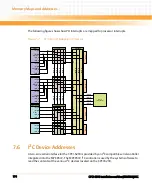
Page 174: ... to read the contents of the various I2C devices located on the CPCI 6200 Figure 7 2 PCI Interrupt Mapping to Processor Primary INTA_N INTB_N INTC_N INTD_N Secondary INTA_N INTB_N INTC_N INTD_N Primary INTA_N INTB_N INTC_N INTD_N Secondary INTA_N INTB_N INTC_N INTD_N CPCI INTA_N INTB_N INTC_N INTD_N INTA_N INTB_N INTC_N 8572 Processor INTA_N INTB_N INTC_N INTD_N Tsi384 PCI 1 Tsi384 PCI 2 Tsi384 PC...

Page 175: ...A4 010 256 x 8 DDR3 memory bank 2 SPD1 0xA6 011 64K x 8 User configuration 1 0xA8 0xAA 100 512 x 8 RTM VPD off board configuration 0xAC 110 64K x 8 User configuration 2 0xAE 111 8K x 8 VPD on board configuration 0xD0 N A N A M41T83 real time clock Bus 3 0x4C or 0x98 NA N A ADT7461 temperature sensor 0xA0 000 64K x 8 User configuration 0xA2 001 64K x 8 VPD on board configuration 0xA4 010 64K x 8 Sy...

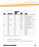
Page 176: ...Devices PCI Bus Device Number Field AD Line for IDSEL PCI Device or Slot Device Slot INT to MPC8572 IRQ INTA INTB INTC INTD PCI1 Tsi384 0b0_0000 20 PMC1 Primary IRQ1 IRQ2 IRQ3 IRQ0 0b0_0001 21 PMC1 Secondary IRQ2 IRQ3 IRQ0 IRQ1 PCI2 Tsi384 0b0_0000 22 PMC2 Primary IRQ0 IRQ1 IRQ2 IRQ3 0b0_0001 23 PMC2 Secondary IRQ1 IRQ2 IRQ3 IRQ0 PCI3 Tsi384 0b0_0010 18 CPCI CPLD IRQ2 IRQ3 IRQ0 IRQ1 PCI4 Tsi381 0b...

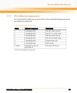
Page 177: ...2 PCI Arbitration Assignments PCI Bus Arbitration Assignment PCI Master s 1 Tsi384 REQ GNT 0 PMC site 1 primary master 1 Tsi384 REQ GNT 1 PMC site 1 secondary master 2 Tsi384 REQ GNT 0 PMC site 2 primary master 2 Tsi384 REQ GNT 1 PMC site 2 secondary master 3 Tsi384 REQ GNT 0 PCI6466 primary Side 4 Tsi381 REQ GNT 0 USB Controller CPCI Bus PCI6466 Secondary Side REQ GNT 6 0 Backplane CPCI Devices1 ...

Page 178: ...Memory Maps and Addresses CPCI 6200 Installation and Use 6806800J66C 178 ...

Page 179: ...Appendix A CPCI 6200 Installation and Use 6806800J66C 179 AReplacing the Battery A 1 Battery Location For information on the battery s functional description see RTC Battery on page 91 RTC Battery ...

Page 180: ...tery are exactly the same battery models If the respective battery model is not available contact your local Emerson sales representative for the availability of alternative officially approved battery models PCB and Battery Holder Damage Removing the battery with a screw driver may damage the PCB or the battery holder Do not use a screw driver to remove the battery from its holder Data Loss Insta...

Page 181: ...can also visit http www emersonnetworkpower com embeddedcomputing Navigate to Solution Services Technical Documentation Search Use the search field to look for the appropriate publication This Web site provides the up to date copies of Emerson product documentation Table B 1 Related Publications Document Title and Source Publication Number CPCI 6200 Quick Start Guide 6806800J85 CPCI 6200 Safety No...

Page 182: ...a4 pdf Analog Devices Inc http www analog com ADT7461 Temperature Monitor ADT7461 Rev B Atmel Corporation http www atmel com 2 Wire Serial EEPROM 32K 4096 x 8 64K 8192 x 8 AT24C32C AT24C64C 5174B SEEPR 12 06 http www atmel com dyn resources prod_documents doc5174 pdf 2 Wire Serial EEPROM 512K 65 536 x 8 Rev 1116K SEEPR 1 04 http www atmel com dyn resources prod_documents doc1116 pdf Broadcom http ...

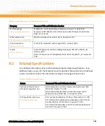
Page 183: ... 16 Byte FIFO s October 2006 Tundra www tundra com Tsi384 PCI Express to PCI PCI X Bridge Data Book 80E1000_MA001_06 October 2007 Tsi381 PCI Express to PCI Bridge Data Book 80F1100_MA001_05 December 2007 Table B 2 Manufacturers Publications continued Company Document Title and Publication Number Table B 3 Related Specifications Source Document Title and Publication Number Institute of Electrical a...

Page 184: ...PCI System Management Specification PICMG 2 9 R 1 0 CPCI Packet Switching Backplane Specification PICMG 2 16 R1 0 Universal Serial Bus http www usb org developers docs Universal Serial Bus Specification Revision 2 0 April 27 2000 VITA Standards Organization http www vita com PPMC ANSI VITA 32 2003 PCI X on PMC ANSI VITA 39 2003 Table B 3 Related Specifications continued Source Document Title and P...

Page 185: ...ersonnel trained by Emerson or persons qualified in electronics or electrical engineering areauthorizedtoinstall removeormaintaintheproduct Theinformationgiveninthismanual is meant to complete the knowledge of a specialist and must not be used as replacement for qualified personnel Keep away from live circuits inside the equipment Operating personnel must not remove equipment covers Only factory a...

Page 186: ...ompliance is maintained Installed blades must have the face plates installed and all vacant slots in the shelf must be covered Forapplicationswherethisproductisprovidedwithoutaface plate orwherethefaceplatehas been removed your system chassis enclosure must provide the required electromagnetic interference EMI shielding to maintain EMC compliance Board products are tested in a representative syste...

Page 187: ...hat is mounted at product delivery may cause data loss since other battery types may be specified for other environments or may have a shorter lifetime Only use the same type of lithium battery as is already installed PCB and Battery Holder Damage Removing the battery with a screw driver may damage the PCB or the battery holder Do not use a screw driver to remove the battery from its holder Produc...

Page 188: ...e LED is permanently illuminated before removing the product Data Loss Removing the RTM with the system power on and the blue LED on the front blade still flashing causes data loss Before removing the RTM from a powered system power down the slot and the front blade s payload by opening the lower handle of the front blade and wait until the blue LED is permanently ON ...

Page 189: ...e für Sie zuständige Geschäftsstelle von Emerson Das Produkt wurde entwickelt um die Sicherheitsanforderungen für SELV Geräte nach der Norm EN 60950 1 für informationstechnische Einrichtungen zu erfüllen Die Verwendung des Produkts in einer anderen Anwendung erfordert eine Sicherheitsüberprüfung für diese spezifische Anwendung Einbau Wartung und Betrieb dürfen nur von durch Emerson ausgebildetem o...

Page 190: ...gemäß den FCC Richtlinien Abschnitt 15 bzw EN 55022 Klasse A Diese Grenzwerte sollen einen angemessenen Schutz vor Störstrahlung beim Betrieb des Produkts in Geschäfts Gewerbe sowie Industriebereichen gewährleisten Das Produkt arbeitet im Hochfrequenzbereich und erzeugt Störstrahlung Bei unsachgemäßem Einbau und anderem als in diesem Handbuch beschriebenen Betrieb können Störungen im Hochfrequenzb...

Page 191: ...betrieben wird Sobald Sie das Produkt oder seine Standardkonfiguration verändern müssen Sie dafür sorgen dass alle relevanten Richtlinien eingehalten werden System Installation Beschädigung von Schaltkreisen Elektrostatische Entladung und unsachgemäßer Ein und Ausbau des Produktes kann Schaltkreise beschädigen oder ihre Lebensdauer verkürzen Bevor Sie das Produkt oder elektronische Komponenten ber...

Page 192: ...n Lithium Batterien kann zu gefährlichen Explosionen führen Wenn SIe die Lithium Batterie auf dem Produkt austauschen stellen Sie sicher dass die alte und die neue Batterie vom gleichen Typ sind Ist der Batterietyp nicht verfügbar wenden Sie sich an Emerson um herauszufinden welcher Batterietyp offiziell alternativ verwendet werden darf Hot Swap Datenverlust Wenn Sie das Produkt ausbauen obwohl di...

Page 193: ...ector J3 50 CPCI user I O connector J5 51 DDR3 memory module 60 Ethernet connector J6 58 front panel 46 front panel latch P1 59 memory module XJ1 and XJ2 60 onboard 47 PCI Express expansion connector J17 62 serial port J16 59 USB 58 conventions 18 CPCI 50 CPCI 6200 configuring 35 features 21 installing 39 removing 41 D DUART interface 78 E ethernet interface 75 F features 21 front panel 46 LED 67 ...

Page 194: ...ts J12 J22 connectors 905 54 J13 J23 connectors 905 55 J14 J24 connectors 905 56 PMC installing 32 PMC module installing 32 PMC sites 80 processor 73 programmable devices 93 R removing baseboard 41 board 41 CPCI 6200 41 single board computer 41 replacing battery 179 requirements environmental 30 operating 30 reset timing 90 S serial interface 73 serial number location 27 single board computer remo...

Page 195: ......

Page 196: ...service marks of Emerson Electric Co All other product or service names are the property of their respective owners 2009 Emerson Electric Co Emerson Network Power The global leader in enabling Business Critical Continuity AC Power Systems Connectivity DC Power Systems Embedded Computing Embedded Power Integrated Cabinet Solutions Outside Plant Power Switching Control Precision Cooling Services Sit...

Reviews: