Embedian, Inc.
1
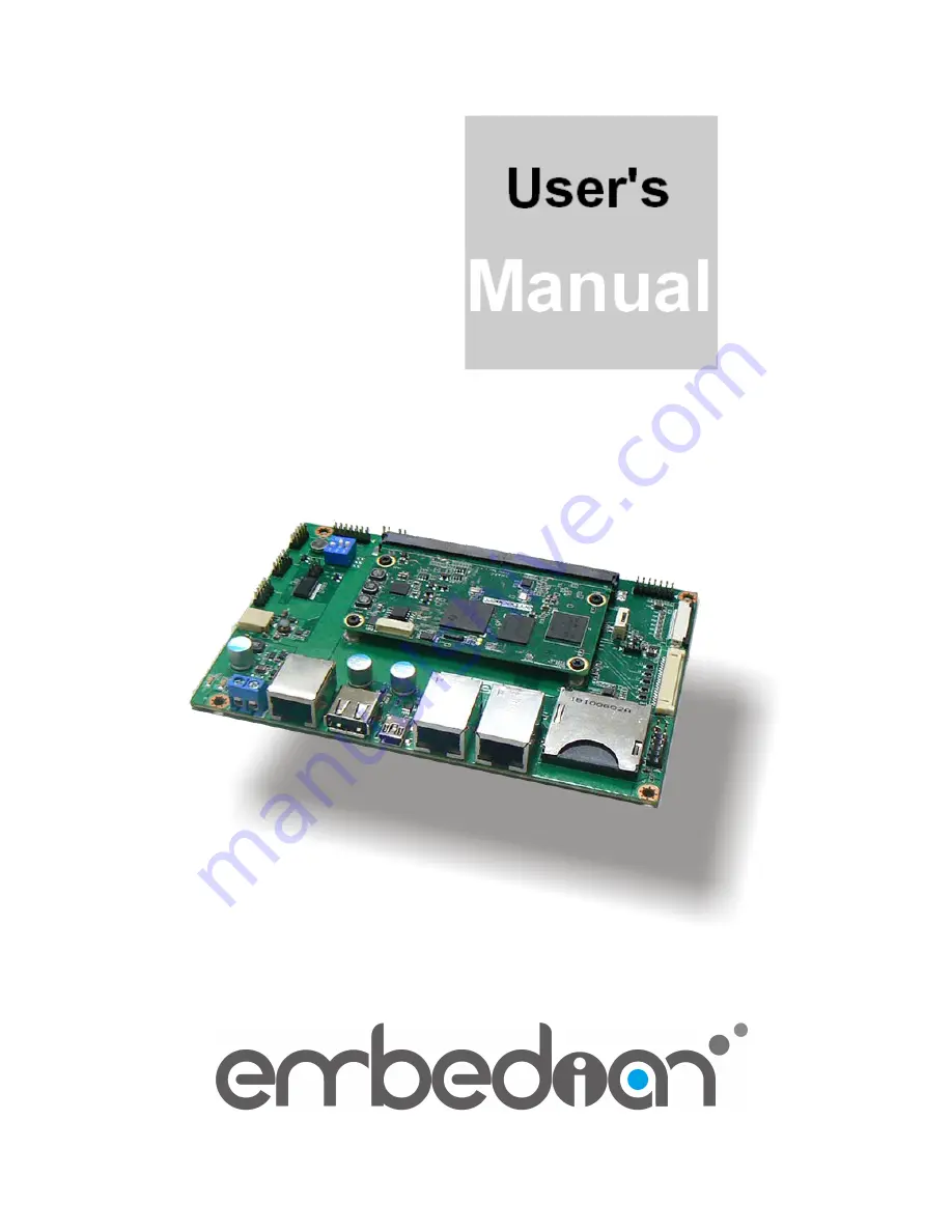
SMART-BEE User’s Manual Document Revision v.1.2
SMARC T335X Evaluation Carrier
SMART-BEE
Page 1: ...Embedian Inc 1 SMART BEE User s Manual Document Revision v 1 2 SMARC T335X Evaluation Carrier SMART BEE...
Page 2: ...sion 1 0 2013 6 21 Initial Release 1 1 2014 4 17 Update to SMARC T335X Hardware Revision 00B0 1 SPI_D0 and SPI_D1 interchanged 2 LCD_BKLT_PWM and GPIO1 interchanged 3 Change Baseboard name from SMARTB...
Page 3: ...BEDIAN Trademarks The following lists the trademarks of components used in this board ARM is a registered trademark of ARM Limited Android is a registered trademark of Google Linux is a registered tra...
Page 4: ...t Technical Support Technicians and engineers from EMBEDIAN and or its subsidiaries and official distributors are available for technical support We are committed to making our product easy to use and...
Page 5: ...TCHES 24 FIGURE 6 SWITCH LOCATIONS 24 2 3 LEDS 26 FIGURE 7 LED LOCATIONS 26 CHAPTER 3 HEADERS AND CONNECTORS 28 3 1 CONNECTORS 28 FIGURE 8 CONNECTOR LOCATIONS 28 FIGURE 9 24 BIT SINGLE PIXEL TRANSMISS...
Page 6: ...new terms variables and document titles monospaced type Filenames pathnames and code examples Embedian Information Document Updates Please always check the product specific section on the Embedian sup...
Page 7: ...BEE User s Manual Document Revision v 1 2 Additional Resources Please also refer to the most recent SMARC T335x User s Manual and TI AM335x processor reference manual and related documentation for ad...
Page 8: ...n v 1 2 Introduction This Chapter gives background information on the SMART BEE Evaluation Carrier Section include SMARC T335X Evaluation Carrier Goals Feature Set Overview Block Diagram Peripheral Ov...
Page 9: ...ent environments prior to use in customer designed applications It can also be used together with SMARC T335X as an application ready 3 5 inch single board computer The SMARC T335X Evaluation Carrier...
Page 10: ...with integrated magnetics On board I2S Audio Codec RS232 support for 3 SMARC serial ports one can be configured as RS422 RS485 CAN Bus support 1 SPI 2 and I2C 2 Header Boot Option Switch SD Card slot...
Page 11: ...O connectors are shown in orange Embedian defined wired I O connectors and headers are shown in red Industry standard mezzanine and slot format connectors are shown in blue ICs on the board are shown...
Page 12: ...Embedian Inc 12 SMART BEE User s Manual Document Revision v 1 2 Figure 1 SMARC T335X Evaluation Carrier Block Diagram Details for this diagram will be explained in the following chapters...
Page 13: ...sion v 1 2 1 4 Peripheral Overview The following diagram shows the function of all peripherals including of connectors headers configuration jumpers and other important features on the SMARC T335X Eva...
Page 14: ...on v 1 2 1 5 Layout Diagram The following section shows the physical location and reference designator of connectors configuration jumpers and other important features on the SMARC T335X Evaluation Ca...
Page 15: ...ion v 1 2 1 6 Mounting Holes Mechanical Drawing Figure 4 shows the mounting holes information of SBC SMART MEN The diameter of mounting hole is 3 2mm and the diameter of the ring is 6mm Figure 4 SBC S...
Page 16: ...bedded EEPROM Specification Rev 1 0 August 2010 www picmg org SD Specifications Part 1 Physical Layer Simplified Specification Version 3 01 May 18 2010 2010 SD Group and SD Card Association Secure Dig...
Page 17: ...s April 15 2013 rev F AM335x Schematic Checklist Oct 31 2011 AM335x ARM Cortex A8 Microprocessors MPUs Technical References Manual April 15 2013 rev H AM335x Power Consumption Summary Oct 31 2011 1 7...
Page 18: ...Embedian Inc 18 SMART BEE User s Manual Document Revision v 1 2 Adeneo Embedded Windows Embedded Compact 7 Nucleus QNX...
Page 19: ...Embedian Inc 19 SMART BEE User s Manual Document Revision v 1 2 Jumpers Switches and LEDs This Chapter provides SMART BEE jumpers switches and LEDs information Section include Jumpers Switches LEDs...
Page 20: ...rmation of the jumpers switches and LEDs 2 1 Jumpers The SMART BEE has a number of jumpers that allow you to configure your system to suit your application All use 2mm shorting blocks shunts to select...
Page 21: ...ng for SER0 UART0 JP3 Hardware Reset JP4 External WatchDog Timer 2 1 3 Jumper Settings The following tables describe how the jumper shunts to various configurations JP1 Location on Board G2 JP1 3 3V 5...
Page 22: ...gure your board to match the needs of your application by setting jumpers A jumper is the simplest kind of electric switch It consists of two metal pins and a small metal clip often protected by a pla...
Page 23: ...l Document Revision v 1 2 A pair of needle nose pliers may be helpful when working with jumpers If you have any doubts about the best hardware configuration for your application contact your sales rep...
Page 24: ...cument Revision v 1 2 2 2 Switches The SMART BEE has one switch SW1 that could determine the boot devices 2 2 1 Switch Location The SW1 switch for boot configuration is located at A1 as shown in the f...
Page 25: ...ion v 1 2 2 2 2 List of Booting Device Configuration The table below lists the booting device configuration setting by SW1 SW1 Function 1 2 3 Boot Configuration OFF ON ON Carrier SD Card CN16 ON OFF O...
Page 26: ...he SMART BEE has two LEDs to indicate the 5V and 3 3V power status When power is fine the LED will light on 2 3 1 LEDs Location Figure 7 LED Locations 2 3 2 List of LEDs The table below lists the func...
Page 27: ...Embedian Inc 27 SMART BEE User s Manual Document Revision v 1 2 Connectors and Headers This Chapter gives SMART BEE connectors and headers detail information Section include Connectors Headers...
Page 28: ...2 Chapter 3 Headers and Connectors This section gives SMART BEE connectors and headers detail information 3 1 Connectors Wired connections to the SMARC T335X Evaluation Carrier are described in this...
Page 29: ...Terminal Block CN3 RTC Backup Battery CN4 LAN1 RJ45 Jack with Integrated Magnetic CN5 LAN2 RJ45 Jack with Integrated Magnetic CN6 USB Host Type A Connector CN7 USB OTG mini Type B Connector CN8 LCD L...
Page 30: ...hapters Pinout Legend I Input O Output I O Input or output P Power AI Analogue input AO Analogue output AIO Analogue Input or analogue output OD Open Drain Signal Low level active signal 3 1 3 1 Seria...
Page 31: ...nector Edge Finger Sitara AM335x CPU Type Header Pin Signal Name Function Pin Ball Mode Signal Name 1 NC Not Connected 2 SER3 _RX Receive Data P141 L17 1 UART3_RXD I 3 SER3 _TX Transmit Data P140 L16...
Page 32: ...rsal serial bus port 1 P66 R17 0 USB1_DM IO 3 USB1 Universal serial bus port 0 P65 R18 0 USB1_DP IO 4 USB_G ND USB Ground P Note To protect the external power lines of peripheral devices make sure tha...
Page 33: ...llowing table shows the pin out of the CN7 USB OTG connector CN7 Location on Board E5 USB OTG Mini Type B Connector Edge Finger Sitara AM335x CPU Type Header Pin Signal Name Function Pin Ball Mode Sig...
Page 34: ...ion on Board G5 Gigabit RJ45 Connector Edge Finger Sitara AM335x CPU Type Header Pin Signal Name Function Pin Ball Mode Signal Name 1 GBE_MDI0 Transmit Data P30 From SMSC LAN8720A AO 2 GBE_MDI0 Transm...
Page 35: ...3 AO 3 GBE1_MDI1 Receive Data S65 AI 4 GBE1_MDI2 Transmit Data S66 NC 5 GBE1_MDI2 Transmit Data S68 NC 6 GBE1_MDI1 Receive Data S69 AI 7 GBE1_MDI3 Receive Data S71 NC 8 GBE1_MDI3 Receive Data S72 NC L...
Page 36: ...Type Header Pin Signal Name Function Pin Ball Mode Signal Name 1 SDIO_CD SDIO_D3 SD Insert Detect SD receive trans mit data P35 P42 U14 F17 7 0 GPIO1 18 MMC0_ DAT3 I IO 2 SDIO_CMD SD receive response...
Page 37: ...tch 0 5mm Top Contact Edge Finger Sitara AM335x CPU Type Header Pin Signal Name Function Pin Ball Mod e Signal Name 1 GND Ground P 2 LCD_PCK Pixel Clock S123 V5 0 LCD_ PCLK O 3 LCD_HS Horizontal Sync...
Page 38: ...Type Header Pin Signal Name Function Pin Ball Mod e Signal Name 12 GND Ground P 13 LCD_GREEN2 Green Data S104 T2 0 LCD_ DATA5 O 14 LCD_GREEN3 S105 T3 0 LCD_ DATA6 O 15 LCD_GREEN4 S106 T4 0 LCD_ DATA7...
Page 39: ..._ DATA17 O 21 LCD_BLUE3 S96 U4 0 LCD_ DATA11 O 22 LCD_BLUE4 S97 V2 0 LCD_ DATA12 O 23 LCD_BLUE5 S98 V3 0 LCD_ DATA13 O 24 LCD_BLUE6 S99 V4 0 LCD_ DATA14 O 25 LCD_BLUE7 S100 T5 0 LCD_ DATA15 O 26 GND G...
Page 40: ...5LVDS83B interface IC on carrier board The following table shows the pin out of the CN10 LCD LVDS connector CN10 Location on Board H4 LVDS Connector CONN DF14 20P 1 25H Edge Finger Sitara AM335x CPU T...
Page 41: ...VCC 3 3V or 5V P 20 20 VCC 3 3V or 5V P Note CN10 is a 24 bit color depth LVDS signal In the 24 bit single pixel mode the RGB and control inputs shall be transmitted as shown in the following figure...
Page 42: ...PU Type Header Pin Signal Name Function Pin Ball Mode Signal Name 1 BLH Backlight Drive Anode Side From TPS61165 P 2 BLL Backlight Drive Cathode Side From TPS61165 P Note The mating connector is JST B...
Page 43: ...options are available including 1 8MM 2 7mm and 8mm The Evaluation Carrier has captive M2 5 threaded standoffs in the SMARC mounting hole positions The standoffs accept M2 5 screws inserted from above...
Page 44: ...rocessor The following table shows the pin out of the CN19 4 wire resistive connector CN19 Location on Board H3 4 wire Touch Connector 1 0 ZIF FPC SMT V T Edge Finger Sitara AM335x CPU Type Header Pin...
Page 45: ...The following table shows the pin out of the CN3 on module JTAG connector CN3 Location on Board D4 JTAG Connector JST SM10B SRSS TB 1mm pitch R A SMD Header Edge Finger Sitara AM335x CPU Type Header P...
Page 46: ...Embedian Inc 46 SMART BEE User s Manual Document Revision v 1 2 Note The mating connector part number is JST 10SR 3S...
Page 47: ...Embedian Inc 47 SMART BEE User s Manual Document Revision v 1 2 3 2 Headers This section details the header information of SMART BEE Evaluation Carrier 3 2 1 Header Location Figure 10 Header Locations...
Page 48: ...ader CN11 Mic In and Speaker Out Audio Header 3 2 3 Header Pin Assignments The following tables describe the electrical signals available on the connectors of the SMART BEE Each section provides relev...
Page 49: ...SER0 have RTS CTS handshaking and two SER1 and SER3 have TX and RX data only without handshaking The Evaluation Carrier runs SER0 and SER1 through one transceiver and SER3 through a 2nd transceiver T...
Page 50: ...Function Pin Ball Mode Signal Name 1 422_ TX 485_ RX 2 422_ TX 485_ RX 3 SER0 _RX Receive Data P130 E15 0 UART0_RXD I 4 SER0 _RTS Ready to Send P131 E17 0 UART0_ RTSN O 5 SER0 _TX Transmit Data P129 E...
Page 51: ...rd A3 RS232 Header HEADER DIP 10 2P 180D MALE 2 0mm Edge Finger Sitara AM335x CPU Type Header Pin Signal Name Function Pin Ball Mode Signal Name 1 NC 2 NC 3 SER1 _RX Receive Data P135 K18 1 UART2_RXD...
Page 52: ...SN65HVD251D transceiver The following table shows the pin out of the CN15 CAN Bus header CN15 Location on Board A2 CAN Bus Header HEADER DIP 10 2P 180D MALE 2 0mm Edge Finger Sitara AM335x CPU Type H...
Page 53: ...Header HEADER DIP 14 2P 180D MALE 2 0mm Edge Finger Sitara AM335x CPU Type Header Pin Signal Name Function Pin Ball Mode Signal Name 1 VDD_ GPIO P 2 GND P 3 GPIO0 Camera 0 Power Enable P108 J17 7 GPI...
Page 54: ...ge Finger Sitara AM335x CPU Type Header Pin Signal Name Function Pin Ball Mode Signal Name 10 GPIO9 CAN1 Error signal active low input P117 V12 7 GPIO2 1 I O 11 GPIO4 HD Audio Reset P112 U6 7 GPIO2 4...
Page 55: ...Function Pin Ball Mode Signal Name 1 Reserved 2 SPI1_ CS0 SPI1 Master Chip Select 0 output P54 C12 3 SPI1_CS0 O 3 SPI0_ CS1 SPI0 Master Chip Select 1 output P31 C15 0 SPI0_CS1 O 4 SPI1_ CS1 SPI1 Mast...
Page 56: ...MISO SPI1 Master Data input input to CPU output from SPI device P57 B13 3 SPI1_D0 I 11 I2C_GP_ CK General purpose I2C bus clock S48 D15 3 I2C1_SCL OD 12 I2C_LCD _GK LCD display I2C bus clock S139 D17...
Page 57: ...o mic In and headset speaker out header is located at CN11 The following table shows the pin out of the CN11 CN11 Location on Board H5 Audio Header HEADER DIP 10 2P 180D MALE 2 54mm Edge Finger Sitara...
Page 58: ...ger Sitara AM335x CPU Type Header Pin Signal Name Function Pin Ball Mode Signal Name 9 HP_OUT_ L Left channel of headset speaker out From TLV320AIC3016 Audio Codec 10 HP_OUT_ LR HPLCOM Signal of AIC31...
Page 59: ...Inc 59 SMART BEE User s Manual Document Revision v 1 2 I2C0 Devices and Carrier EEPROM Format This Chapter points out the I2C0 device information Section include I2C Devices on Carrier Carrier EEPROM...
Page 60: ...l on the I2C_PM I2C0 bus and are operated at 3 3V Those devices and their address details are listed in the following table Device Description Address 7 bit Address 8 bit Notes Read Write I2C_PM Bus 1...
Page 61: ...the PICMG EEEP Embedded EEPROM Specification If developers have more than one carrier boards all using SMARC T335X as the core module it is recommended to have an EEPROM on carrier The advantage for...
Page 62: ...Bit 14 13 Pin Direction 1 0 Output 01 Input 11 BDIR Bits 12 7 Reserved Bit 6 Slew Rate 0 Fast 1 Slow Bit 5 Rx Enable 0 Disabled 1 Enabled Bit 4 Pull Up Dn Select 0 Pulldown 1 PullUp Bit 3 Pull Up DN...
Page 63: ...Inc 63 SMART BEE User s Manual Document Revision v 1 2 Quick Start Guide The purpose of this chapter is to provide a quick start guide so that developers can easily get the board up and running in few...
Page 64: ...s of configuring installing and developing SMARC T335X This guide was written to be as clear as possible and to provide only the details necessary to get you up and running For more in depth informati...
Page 65: ...s Manual Document Revision v 1 2 Step3 Wired the console and Ethernet cable Connect the DB9 to RJ 45 console debug cable from CN14 of the device to your PC and the Ethernet cable from LAN1 CN4 of the...
Page 66: ...he device Apply 5V to CN2 connector of the device If you see the LED light on that means the wiring is correct Do not need to worry about the mis wiring because the device has mis wiring protection Yo...