7
Overview of the Kit
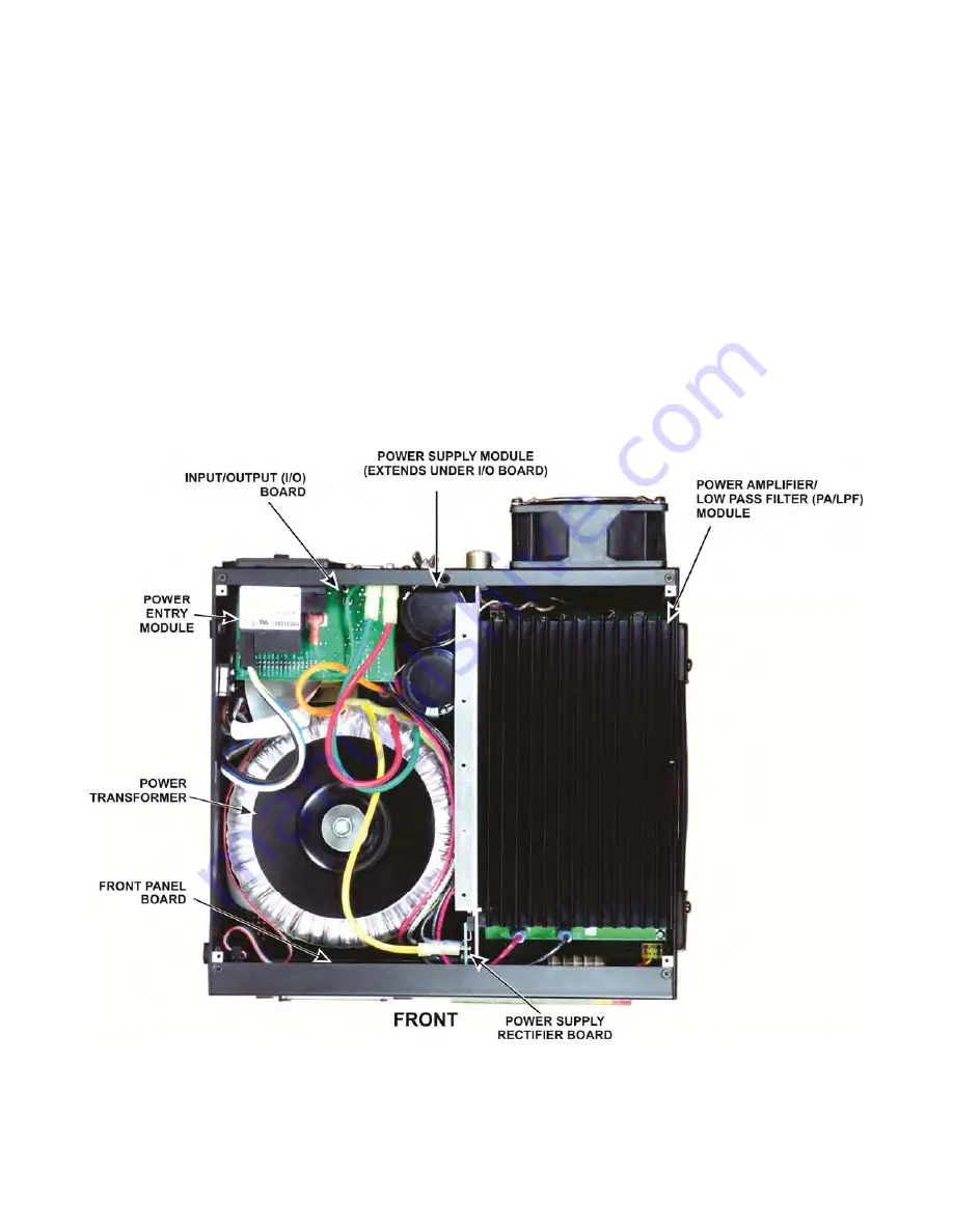
Figure 4 is a top view of the KPA500 with the top cover removed. The chassis is divided into two major areas
by a bracket (called the Z-bracket due to its shape) that runs down the middle from front to back. The RF
circuitry is on the right in this view, and the power supply is on the left.
The RF circuitry is supplied assembled, factory tested and aligned. It consists of a “sandwich” of two boards; a
power amplifier board mounted on the heat sink and an output low pass filter board below it.
On the left is the power supply, dominated by the toroidal power transformer. Largely hidden by the I/O board is
the power supply module that contains the regulators and other components of the power supply except the
rectifiers. The rectifiers are mounted on a separate board near the front that uses the Z-bracket for a heat sink.
The I/O board provides the circuitry needed by the RS232, AUX and other rear panel interface connectors.
The front panel board contains all the control circuitry, including the circuitry required by the front panel
switches and displays. The front panel board is connected to the I/O board by a ribbon cable that runs alongside
the power transformer.
Figure 4. Assembled KPA500 with Top Cover Removed.


