background image

EM78P447N


8-Bit Microcontroller with OTP ROM


22 


Product Specification (V1.1) 03.30.2005


(This specification is subject to change without further notice) 


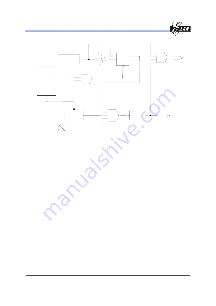
Voltage

Detector

Power-on

Reset

WDTE

Setup Time

VDD

D

Q

CLK

CLR

CLK

RESET

WDT Timeout

WDT

/RESET

Oscillator


Fig. 8  Controller Reset Block Diagram 


4.6 Interrupt 

The EM78P447N has two interrupts listed below: 

(1) TCC overflow interrupt 

(2) External interrupt (/INT pin). 

R3F is the interrupt status register that records the interrupt requests in the relative 
flags/bits.  IOCF is the interrupt mask register.  The global interrupt is enabled by the 
ENI instruction and is disabled by the DISI instruction.  When one of the interrupts 
(enabled) occurs, the next instruction will be fetched from address 001H.  Once in the 
interrupt service routine, the source of an interrupt can be determined by polling the flag 
bits in R3F.  The interrupt flag bit must be cleared by instructions before leaving the 
interrupt service routine and before interrupts are enabled to avoid recursive interrupts. 

The flag (except ICIF bit) in the Interrupt Status Register (R3F) is set regardless of the 
status of its mask bit or the execution of ENI.  Note that the outcome of R3F are the 
logic AND of R3F and IOCF (refer to Fig. 9).  The RETI instruction ends the interrupt 
routine and enables the global interrupt (the execution of ENI). 

When an interrupt is generated by the INT instruction (enabled), the next instruction will 
be fetched from address 002H. 

Summary of Contents for 8-Bit Microcontroller with OTP ROM EM78P447N

Page 1: ...EM78P447N 8 Bit Microcontroller with OTP ROM Product Specification DOC VERSION 1 1 ELAN MICROELECTRONICS CORP March 2005...

Page 2: ...d or copied only in accordance with the terms of such agreement ELAN Microelectronics products are not intended for use in life support appliances devices or systems Use of ELAN Microelectronics produ...

Page 3: ...rol Register 11 4 2 3 IOC5 IOC7 I O Port Control Register 12 4 2 4 IOCB Wake up Control Register for Port6 12 4 2 5 IOCE WDT Control Register 13 4 2 6 IOCF Interrupt Mask Register 14 4 3 TCC WDT Presc...

Page 4: ...TICS 34 6 1 DC Electrical Characteristic 34 6 2 AC Electrical Characteristic 35 6 3 Device Characteristic 36 APPENDIX A Package Types 50 B Package Information 50 Specification Revision History Doc Ver...

Page 5: ...iter to easily program his development code 2 FEATURES Operating voltage range 2 5V 5 5V Operating temperature range 40 C 85 C Operating frequency rang base on 2 clocks Crystal mode DC 20MHz at 5V DC...

Page 6: ...n pins 2 programmable R option pins Package types 20 pin DIP 300mil EM78P447NDP 20 pin SOP 300mil EM78P447NDM 24 pin Skinny DIP 300mil EM78P447NCK 24 pin SOP 300mil EM78P447NCM 28 pin DIP 600mil EM78P...

Page 7: ...P447NBWM 1 2 3 4 5 6 7 8 9 10 11 12 14 13 26 25 24 23 22 21 20 19 18 17 29 30 27 28 P55 P54 P56 P57 15 16 31 32 DIP SOP P54 TCC VDD Vss INT P50 P51 P53 P60 P61 P62 P52 RESET OSCI OSCO P77 P76 P75 P74...

Page 8: ...an have open drain output by software control P70 and P71 can also be defined as the R option pins INT 5 I External interrupt pin triggered by falling edge VSS 4 Ground NC 3 No connection Table 2 EM78...

Page 9: ...trol P76 P77 can have open drain output by software control P70 and P71 can also be defined as the R option pins INT 7 I External interrupt pin triggered by falling edge VSS 6 Ground NC 5 No connectio...

Page 10: ...0 10 I O P60 are bi directional I O pins This can be pulled high internally by software control P71 P77 11 17 I O P74 P77 are bi directional I O pins P74 P75 can be pulled high internally by software...

Page 11: ...are stack are 10 bit wide The structure is depicted in Fig 3 Generating 1024 13 bits on chip OTP ROM addresses to the relative programming instruction codes One program page is 1024 words long R2 is s...

Page 12: ...truction that would change the contents of R2 Such instruction will need one more instruction cycle A7 A0 On chip Program Memory 000H FFFH 001H Hardware Vector User Memory Space Software Vector Reset...

Page 13: ...rve 05 R5 Port5 IOC5 I O Port Control Register 06 R6 Port6 IOC6 I O Port Control Register 07 R7 Port7 IOC7 I O Port Control Register 08 General Register Reserve 09 General Register Reserve 0A General...

Page 14: ...Program memory page Address 0 0 Page 0 000 3FF 0 1 Page 1 400 7FF 1 0 Page 2 800 BFF 1 1 Page 3 C00 FFF Bit 4 T Time out bit Set to 1 with the SLEP and WDTC commands or during power up and reset to 0...

Page 15: ...y instruction but cannot be set by instruction IOCF is the interrupt mask register Note that reading R3F will obtain the result of the R3F logic AND and IOCF 4 2 Special Purpose Registers 4 2 1 A Accu...

Page 16: ...the relative I O pin as output IOC5 and IOC7 registers are both readable and writable 4 2 4 IOCB Wake up Control Register for Port6 7 6 5 4 3 2 1 0 WUE7 WUE6 WUE5 WUE4 WUE3 WUE2 WUE1 WUE0 Bit 7 WUE7 C...

Page 17: ...he controller enters into SLEEP2 mode on the high to low transition and is enabled controller is awakened from SLEEP2 mode on low to high transition In order to ensure the stable output of the oscilla...

Page 18: ...EXIE EXIF interrupt enable bit 0 disable EXIF interrupt 1 enable EXIF interrupt Bit 0 TCIE TCIF interrupt enable bit 0 disable TCIF interrupt 1 enable TCIF interrupt Bits 1 2 and 4 7 Not used Individu...

Page 19: ...e without prescaler Referring to Fig 6 CLK Fosc 2 or CLK Fosc 4 selection is determined by the CODE Option bit CLK status CLK Fosc 2 is used if CLK bit is 0 and CLK Fosc 4 is used if CLK bit is 1 If T...

Page 20: ...on Port 6 P74 and P75 Each I O pin can be defined as input or output pin by the I O control register IOC5 IOC7 The I O registers and I O control registers are both readable and writable The I O inter...

Page 21: ...of R3 are cleared Upon power on the upper 2 bits of R4 are cleared The bits of CONT register are set to all 1 except bit 6 INT flag IOCB register is set to 1 disable P60 P67 wake up function Bits 3 an...

Page 22: ...will trigger a controller reset Table 6 Usage of Sleep1 and Sleep2 Mode Usage of Sleep1 and Sleep2 Mode SLEEP2 SLEEP1 a Before SLEEP a Before SLEEP 1 Set Port6 or P74 or P75 Input 1 Execute SLEP inst...

Page 23: ...P P Bit Name C67 C66 C65 C64 C63 C62 C61 C60 N A IOC6 Power On 1 1 1 1 1 1 1 1 RESET and WDT 1 1 1 1 1 1 1 1 Wake Up from Pin Change P P P P P P P P Bit Name C77 C76 C75 C74 C73 C72 C71 C70 N A IOC7 P...

Page 24: ...ISR Power On U U U U 0 U U 0 RESET and WDT U U U U 0 U U 0 Wake Up from Pin Change U U U U P U U P Bit Name WUE7 WUE6 WUE5 WUE4 WUE3 WUE2 WUE1 WUE0 0x0B IOCB Power On 1 1 1 1 1 1 1 1 RESET and WDT 1 1...

Page 25: ...ocessor to wake up Table 8 shows the events that may affect the status of T and P Table 8 The Values of RST T and P after RESET Reset Type T P Power on 1 1 RESET during Operating mode P P RESET wake u...

Page 26: ...ISI instruction When one of the interrupts enabled occurs the next instruction will be fetched from address 001H Once in the interrupt service routine the source of an interrupt can be determined by p...

Page 27: ...illator mode low XTAL LXT oscillator mode and External RC oscillator mode ERC oscillator mode User can select one of them by programming MS HLF and HLP in the Code Option Register Table 10 depicts how...

Page 28: ...10 below In most applications Pin OSCI and Pin OSCO can be connected with a crystal or ceramic resonator to generate oscillation Fig 12 depicts such circuit The same thing applies whether it is in the...

Page 29: ...f the resistor Rext the capacitor Cext and even by the operation temperature Moreover the frequency also changes slightly from one chip to another due to the manufacturing process variation In order t...

Page 30: ...0 pF 100k 21 KHz 21 KHz NOTE 1 Measured on DIP packages 2 For design reference only 4 8 CODE Option Register The EM78P447N has one CODE option word that is not a part of the normal program memory The...

Page 31: ...447NA Bit 5 HLF XTAL frequency selection 0 XTAL2 type low frequency 32 768KHz 1 XTAL1 type high frequency This bit will affect system oscillation only when Bit4 OSC is 1 When OSC is 0 HLF must be 0 NO...

Page 32: ...required to assist in solving power up problems 4 10 External Power On Reset Circuit The circuit shown in Fig 16 implements an external RC to produce the reset pulse The pulse width time constant sho...

Page 33: ...ower Vdd is taken off but residue voltage remains The residue voltage may trips below Vdd minimum but not to zero This condition may cause a poor power on reset Fig 16 and Fig 17 show how to build the...

Page 34: ...S JBC JZ JZA DJZ DJZA instructions which were tested to be true Also execute within two instruction cycles the instructions that are written to the program counter Case A is selected by the CODE Optio...

Page 35: ...None 0 0000 0001 rrrr 001r IOR R IOCR A None Note1 0 0000 0010 000 0020 TBL R2 A R2 Bits 8 9 of R2 unchanged Z C DC 0 0000 01rr rrrr 00rr MOV R A A R None 0 0000 1000 000 0080 CLRA 0 A Z 0 0000 11rr...

Page 36: ...A skip if zero None 0 0111 11rr rrrr 07rr JZ R R 1 R skip if zero None 0 100b bbrr rrrr 0xxx BC R b 0 R b None Note2 0 101b bbrr rrrr 0xxx BS R b 1 R b None Note3 0 110b bbrr rrrr 0xxx JBC R b if R b...

Page 37: ...her notice 4 13 Timing Diagram RESET Timing CLK 0 CLK RESET NOP Instruction 1 Executed Tdrh TCC Input Timing CLKS 0 CLK TCC Ttcc Tins AC Testing Input is driven at 2 4V for logic 1 and 0 4V for logic...

Page 38: ...1 A VIH1 Input High Voltage VDD 5V Ports 5 6 7 2 0 V VIL1 Input Low Voltage VDD 5V Ports 5 6 7 0 8 V VIHT1 Input High Threshold Voltage VDD 5V RESET TCC INT 2 0 V VILT1 Input Low Threshold Voltage VD...

Page 39: ...Fosc 10MHz Crystal type CLKS 0 output pin floating WDT enabled 2 8 5 0 mA 6 2 AC Electrical Characteristic Ta 40 C 85 C VDD 5V 5 VSS 0V Symbol Parameter Conditions Min Typ Max Unit Dclk Input CLK dut...

Page 40: ...ein are not guaranteed for it accuracy In some graphic the data maybe out of the specified warranted operating range Vih Vil Input pins with schmitt inverter 0 0 5 1 1 5 2 2 5 3 3 5 4 4 5 5 5 5 Vdd Vo...

Page 41: ...TP ROM Product Specification V1 1 03 30 2005 37 This specification is subject to change without further notice Voh Ioh VDD 5V 25 20 15 10 5 0 0 1 2 3 4 5 Voh Volt Ioh mA Fig 18 Port5 Port6 and Port7 V...

Page 42: ...ROM 38 Product Specification V1 1 03 30 2005 This specification is subject to change without further notice Voh Ioh VDD 3V 10 8 6 4 2 0 0 0 5 1 1 5 2 2 5 3 Voh Volt Ioh mA Fig 19 Port5 Port6 and Port...

Page 43: ...OM Product Specification V1 1 03 30 2005 39 This specification is subject to change without further notice Vol Iol VDD 5V 0 10 20 30 40 50 60 70 80 90 0 1 2 3 4 5 6 Vol Volt Iol mA Fig 20 Port5 and Po...

Page 44: ...M 40 Product Specification V1 1 03 30 2005 This specification is subject to change without further notice Vol Iol VDD 3V 0 5 10 15 20 25 30 35 40 0 0 5 1 1 5 2 2 5 3 Vol Volt Iol mA Fig 21 Port5 and P...

Page 45: ...OTP ROM Product Specification V1 1 03 30 2005 41 This specification is subject to change without further notice Vol Iol 5V 0 10 20 30 40 50 60 70 80 90 100 0 1 2 3 4 5 6 Vol Volt Iol mA Fig 22 Port7 V...

Page 46: ...TP ROM 42 Product Specification V1 1 03 30 2005 This specification is subject to change without further notice Vol Iol 3V 0 5 10 15 20 25 30 35 40 45 0 0 5 1 1 5 2 2 5 3 Vol Volt Iol mA Fig 23 Port7 V...

Page 47: ...Specification V1 1 03 30 2005 43 This specification is subject to change without further notice WDT Time_out 0 5 10 15 20 25 30 35 2 3 4 5 6 VDD Volt WDT period mS Fig 24 WDT Time Out Period vs VDD Pr...

Page 48: ...30 2005 This specification is subject to change without further notice Cext 100pF Typical RC OSC Frequency 0 0 2 0 4 0 6 0 8 1 1 2 1 4 2 5 3 3 5 4 4 5 5 5 5 VDD Volt Frequency M Hz Fig 25 Typical RC...

Page 49: ...requency vs Temperature R and C are ideal component Four conditions exist with the operating current ICC1 to ICC4 these conditions are as follows ICC1 VDD 3V Fosc 32 kHz 2clock WDT disable ICC2 VDD 3V...

Page 50: ...um ICC1 and ICC2 vs Temperature 15 18 21 24 27 40 20 0 20 40 60 80 Temperature Current uA Fig 28 Maximum Operating Current ICC1 and ICC2 vs Temperature Typical ICC3 and ICC4 vs Temperature 0 5 1 1 5 2...

Page 51: ...40 60 80 Temperature Current mA Fig 30 Maximum Operating Current ICC3 and ICC4 vs Temperature Two conditions exist with the standby current ISB1 and ISB2 these conditions are as follow ISB1 VDD 5V WD...

Page 52: ...urther notice Maximum ISB1 and ISB2 vs Temperature 0 3 6 9 12 15 40 20 0 20 40 60 80 Temperature Current uA Fig 32 Maximum Standby Current ISB1 and ISB2 vs Temperature Operating voltage 40 85 0 5 10 1...

Page 53: ...ication is subject to change without further notice EM78P447N HXT I V 0 0 5 1 1 5 2 2 5 3 0 1 2 3 4 5 6 Volt V I mA Fig 34 EM78P447N I V Curve Operating at 4 MHz EM78P447N LXT I V 0 5 10 15 20 25 30 3...

Page 54: ...28 600 mil EM78P447NAM SOP 28 300 mil EM78P447NAS SSOP 28 209 mil EM78P447NBP DIP 32 600 mil EM78P447NBWM SOP 32 450 mil B Package Information 20 Lead plastic dual inline package DIP 300 mil TITLE PDI...

Page 55: ...24L SKINNY 300MIL PACKAGE OUTLINE DIMENSION Unit mm Scale Free File K24 Material Edtion A Sheet 1 of 1 A2 A1 e 1 12 13 24 Min Normal Max 5 334 0 381 3 175 3 302 3 429 0 203 0 254 0 356 31 750 31 801 3...

Page 56: ...astic dual inline package DIP 600 mil 20 Lead plastic small outline package SOP 300 mil TITLE SOP 20L 300MIL PACKAGE OUTLINE DIMENSION Unit mm Scale Free File SO20 Material Edtion A Sheet 1 of 1 b e S...

Page 57: ...stic small outline package SOP 300 mil TITLE SOP 24L 300MIL PACKAGE OUTLINE DIMENSION Unit mm Scale Free File SO24 Material Edtion A Sheet 1 of 1 b e Symbal A A1 b c E H D L e c Min Normal Max 2 350 2...

Page 58: ...troller with OTP ROM 54 Product Specification V1 1 03 30 2005 This specification is subject to change without further notice 32 Lead plastic small outline package SOP 300 mil 28 Lead Shrink Small Outl...

Reviews: