Command and feedback signals are connected through R1 and
R2 to the input of amplifier A1. Resistors R1, R2, and amplifier
A1’s input resistance form a summing network which permits a
difference potential to be developed across amplifier A1’s input
resistance. The amplitude of this potential is determined by the
polarity and amplitude of the input signals, the input coupling
resistance R1 and R2, and the input resistance of amplifier A1.
Under normal operating conditions, the junction of R1 and R2
is maintained at ‘‘virtual ground’’ within a few millivolts by A1.
Diodes D8 and D9 limit amplitude extremes at the input of A1
to approximately
.5 volt minimum, if the amplifier output
saturates. Amplifier A1 inverts the output signal with respect to
the input signal, permitting gain adjustment to be obtained by a
negative feedback arrangement through resistors R3 and R4.
A portion of the inverted output is allowed to develop across
the input resistance of amplifier A1. This negative feedback
subtracts from the input signal subsequently reducing the gain
of the amplifier.
The output of A1 is used to drive amplifier A2 which in turn pro-
vides the current necessary to drive power transistor Q5 and
Q6. (Shown on the complete schematic diagram Figure 1).
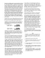
Amplifiers A1 and A2 are of the same type. But amplifier A1’s
gain differs from that of amplifier A2, due to wiring arrange-
ment. Amplifier A1’s gain is essentially the ratio of feedback
to input resistance or:
A1 Gain - Input 1
(Approx. gain of 2)
A1 Gain - Input 2
(Approx. gain of 20)
=
=
R3 +
R1
R2
R4
S
R4a
R4 + R4a
R3 +
R4
S
R4a
R4 + R4a
Amplifier A2 is connected to provide a non-inverting, unity
gain amplifier characteristic. Unity gain amplifiers (gain of 1)
provide isolation between circuits (buffer action) and will per-
mit a source with low current capacity (A1) to drive a heavy
load (Q5 and Q6).
Transistor Q5 and Q6 develop the necessary output current
for the servo coil. Resistors R20 and R20a bias amplifier A2
and establish the 200 MA null current through Q6, D6, the
servo coil, and resistor R26 (the current sensing resistor).
A voltage is developed across R26 directly proportional to the
current through it. The voltage is reduced through voltage
divider action by R23 and R21, and is fed to pin two (2) of the
unity gain amplifier A2 reducing its gain. This gain reduction
(negative feedback) improves the linearity of the driver stage
A2 and the output transistor circuit Q5 and Q6. R25a and
R25b are adjusted to limit the maximum current. When the
voltage across R25a and R25b exceeds the threshold voltage
of D4 and D5, the diodes conduct limiting a further current
rise in the output circuit.
Dither - The dither signal (60 to 400 Hertz) is connected to pin
1 of the plug-in module. A variable resistive divider network
R16 and R18 provide adjustment of the value of the dither.
The dither is applied to pin two (2) of amplifier A2 through
resistor R17. Dither signal is used to keep the servo flapper in
constant motion, thus preventing the flapper from magnetizing
in a locked condition against the orifice. Constant motion of
the flapper will also reduce the effect of silting (the particle
build-up around the orifice).
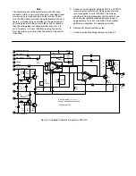
Power Supplies - Four regulated power supplies are
provided on the plug-in module. Refer to the schematic
diagram figure 1. The amplifier section utilizes both a
positive ten (+10) and a negative ten (–10) volt supply for
operation. A positive ten (+10) and a negative ten (–10)
volt supply is also available for external use.
The externally connected supplies may be used for
amplifier control circuitry if desired, thus providing the
control voltage and amplifiers necessary for a complete
system in one plug-in module.
All the regulated supplies operate in a similar manner,
therefore, explanation of only one will be presented.
Upon application of negative nineteen (–19) volts DC to
pin 3 of the plug-in module, Zener Diode Z2 conducts
through R7 establishing a regulated source voltage for
the base of Q2. A portion of this regulated voltage is
applied to Q2 through the voltage divider network of R9,
D2, and R11. Diode D2 and resistor R11 shunt the base
resistance of Q2 and reduce the base drive as the
temperature rises. This reduction in drive prevents
thermal runaway of transistor Q2. Emitter resistor R13
swamps the emitter base junction resistance and
prevents a large increase in emitter current, particularly
at low temperatures. Q2 and R13 act as a variable
voltage dropping resistor for Zener Diode Z4, and
maintain a constant current through Z4 with varying input
voltages. The combined action of Q2 and Z4 provide a
regulated -10 volt source at pin 8 of the plug-in module.
E. Troubleshooting Procedure
Determine if the EM-A-10 module is functional. Refer to
the schematic diagram figure 1 and the pictorial diagram
Figure 2.
Note
The EMP-A-11 power supply or its equivalent must
be used to perform the following test. Minor wiring
changes may be required if an equivalent supply is
used.
1. Remove electrical power from the system.
2. Remove the input signal connections 4, 5, 6, 7, and
8. Tape the wire ends and symbolize to prevent
error.
3. Connect a linear taper, 5000 ohm test potentiometer
as shown in figure 4.
4. Remove the EM-A-10 plug-in module. Use the ohm-
meter on the low ohm scale to check the resistance
of the load as follows:
Connect the ohmmeter between J* - m & n. A read-
ing of approximately 20 ohms is considered normal.
If the reading is normal, reinsert the plug-in module
and proceed with the test.


