MXH932
User’s Guide –
Dolphin Interconnect Solutions
Page 18
PCIe Cable Port Signals
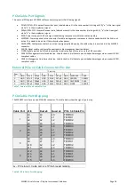
The external PCI Express SFF-8644 cable connector supports the following signals:
•
PETpN/PETnN:
PCI Express Transmitter pairs, labeled where N is the Lane number (starting with 0); “p” is the true signal
while “n” is the complement signal.
•
PERpN/PERnN: PCI Express Receiver pairs, labeled where N is the Lane number
(starting with 0); “p” is the true signal
while “n” is the complement signal.
•
PWR: Power to support AOC and signal conditioning components within the cable assembly.
•
MGTPWR: Power supplied to the connector for cable management components that are needed while the link is not
active. This needs to be active if the subsystem has power.
•
CBLPRSNT#: Cable present detect, an active-low signal pulled-down by the cable when it is inserted into the MXH932
connector.
•
CADDR: Signal used to configure the upstream cable management device address.
•
CINT#: Signal asserted by the cable assembly to indicate a need for service via the CMI controller.
•
CMISDA: Management interface data line. Used for both initial link setup and sideband messages when used with CMI
compliant cables.
•
CMISCL: Management interface clock line. Used for both initial link setup and sideband messages when used with CMI
compliant cables.
External PCIe x4 Cable Connector Pin-Out
Column
Row 9
8
7
6
5
4
3
2
1
D
GND PETn2
PETp2
GND PETn1
PETp1 GND MGTPWR
PWR
C
GND PETn3
PETp3
GND PETn0
PETp0 GND CMISDA
CMISCL
B
GND PERn2 PERp2 GND PERn1 PERp1 GND CBLPRSNT# PWR
A
GND PERn3 PERp3 GND PERn0 PERp0 GND CINT#
CADDR
Table 7; External PCIe x4 cable Pin-Out
PCIe Cable Port Mapping
The MXH932 card have a quad SFF-8644 connector. The table below show the signal / port map.
Table 8 : PCIe Cable Port Mapping
Cable Port
x16
Dual x8
Quad x4
PCIe 3.0 Cable Pin
L0
L0
L0
TX0/RX0
L1
L1
L1
TX1/RX1
L2
L2
L2
TX2/RX2
L3
L3
L3
TX3/RX3
L4
L4
L0
TX0/RX0
L5
L5
L1
TX1/RX1
L6
L6
L2
TX2/RX2
L7
L7
L3
TX3/RX3
L8
L0
L0
TX0/RX0
L9
L1
L1
TX1/RX1
L10
L2
L2
TX2/RX2
L11
L3
L3
TX3/RX3
L12
L4
L0
TX0/RX0
L13
L5
L1
TX1/RX1
L14
L6
L2
TX2/RX2
L15
L7
L3
TX3/RX3
Lx – PCIe lane X, Cable port is ref PCIe bracket marking
1
2
3
4

