Diamond-MM-48-AT User Manual V1.01
Page 31
9. A/D SCAN, FIFO, AND INTERRUPT OPERATION
This chapter describes in detail the interrupt performance of the A/D circuit under all
conditions.
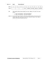
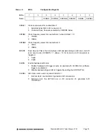
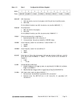
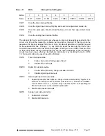
The control bits FIFOEN (FIFO enable), FIFOTH (FIFO threshold), SCANEN (scan enable),
SCNINT (scan interval), and AINTE (A/D interrupt enable) determine the behavior of the
board during A/D conversions with interrupts. Control bits CLKEN and CLKSEL determine
the source of the A/D trigger, either software, on-board counter/timer, or external signal.
In all cases, at the end of an AD conversion A/D data is latched into the FIFO in an
interleaved fashion, first LSB, then MSB. A/D Data is read out of the FIFO with 2 read
operations, first Base + 0 (LSB) and then Base + 1 (MSB).
When SCANEN = 1, each time an A/D trigger occurs, the board will perform an A/D
conversion on all channels in the channel range. The time between A/D conversions is
determined by the setting of the SCNINT bit. When SCANEN = 0, each time an A/D trigger
occurs, the board will perform a single A/D conversion and then advance to the next channel
and wait for the next trigger.
During interrupt operation, if FIFOEN = 1, then the FIFO will fill up with data until it reaches or
exceeds half-full (half-full = 256 samples), and then the interrupt request will occur.
The basic sequence is as follows:
1. A/D trigger command occurs
2. A/D conversion or A/D scan occurs
3. A/D data is stored in the FIFO
4. Interrupt request occurs
5. Interrupt routine extracts data from the FIFO and resets the interrup request
A/D Trigger
The A/D trigger may come from one of three sources as determined by the control bits
CLKEN and CLKSEL:
CLKEN CLKSEL
A/D trigger source
0
0
Software command: write a 1 to ADSTART bit in register 8
0
1
Same as above
1
0
External signal: rising edge on EXTCLK pin on I/O header J3
1
1
Internal; counter/timer 0 controls the A/D conversion timing
A/D Conversion or Scan
Once the A/D trigger occurs, either a single A/D conversion will occur on the current channel,
or an A/D scan will occur on a range of channels selected by the setting of register 2. The
selection is made with the control bit SCANEN:
SCANEN Function
0
Single conversion occurs on the current channel; The internal A/D channel
counter increments after each conversion, so each successive trigger samples
the next channel in the list. At the end of the list, the channel register resets to
the starting channel and the sequence repeats.
1
Scan occurs on all channels in the range programmed in the channel register
(base + 2). The delay between the start of each conversion is determined by the
setting of SCNINT in base + 9: SCNINT = 0 sets a delay of 5
µ
s, and SCNINT = 1
sets a delay of 9.3
µ
s.

