background image

Proceeding :

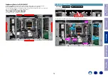
TOP COVER

FRONT PANEL ASSY

RADIATOR ASSY

(1)  Remove the screws.  Remove the STYLE PIN and connectors.

(3)  Remove the connector.  Remove the PUSH RIVET.  Remove the connector.

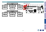
2. RADIATOR ASSY

x8

PUSH RIVET x2

L-AMP

 CONNECT

H2L

PURPLE

H1L

YELLOW

SBL

GRAY

H3L

ORANGE

SL

BROWN

FL

RED

C

BLUE

R-AMP

 CONNECT

FR

RED

SR

BROWN

H3R

ORENGE

H1R

YELLOW

H2R

PURPLE

SBR

GRAY

N5833 N5834

N5842 N5841 PC SHEET

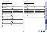
Proceeding :

TOP COVER

BACK PANEL ASSY

(1)  Remove the screws.

(2)  Remove the screws.

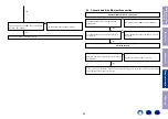
3. BACK PANEL ASSY

Shooting direction: D

Shooting direction: C

View from the bottom

x4

x1

x1

Shooting direction: A

x5

Before Servicing 

This Unit

Electrical

Mechanical

Repair Information

Updating

77

Summary of Contents for AVC-X8500H

Page 1: ...nuals denon com AVRX8500H NA EN index php EU http manuals denon com AVCX8500H EU EN index php AP http manuals denon com AVCX8500H AP ZH index php JP http manuals denon com AVCX8500H JP JA index php Up...

Page 2: ...ONLINE PARTS LIST Accessing the Parts List Searching Part Numbers or Ref Numbers NOTE FOR PARTS LIST SERIAL NUMBER Serial Number Organization SKU Code of this Unit POST SERVICE PRECAUTIONS Initializi...

Page 3: ...c diagrams and parts lists be sure to use the designated parts Be sure to mount parts and arrange the wires as they were originally placed For safety seasons some parts use tapes tubes or other insula...

Page 4: ...PUT CONDITION 4 CIRCUIT AND PARTS ARE SUBJECT TO CHANGE WITHOUT PRIOR NOTICE Electrostatic breakdown of the semi conductors or optical pickup may occur due to a potential differ ence caused by electro...

Page 5: ...art numbers or Ref numbers 1 Enter the part number or Ref number in the search window of the Parts List and press the search button 2 The search results are displayed The name of the sheet in which th...

Page 6: ...al Number Organization The 14 digit serial number that contains the code of the manufacturing plant and the manufacturing date SKU code 14 digits Factory code Cumulative serial number Manufactured Yea...

Page 7: ...etwork related settings NOTE If the unit fails to enter the service mode in step 3 repeat the procedure from step 1 Initializing the device restores the customized settings to the factory settings Wri...

Page 8: ...FRONT HDMI USB SCH29_SMPS SCH30_P AMP1 SCH31_P AMP2 SCH32_SPEAKER SCH33_REG SCH34_232C PHONO SCH35_FRONT PRINTED CIRCUIT BOARDS DIGITAL L AMP CONNECT R AMP CONNECT AUDIO VIDEO FRONT HDMI FRONT USB CON...

Page 9: ...DET FL_CE2 RCOUT KILLIR FLASHERIN FL_CTRL VAUXV H PR H PL VAUXR VAUXL H PR H PL VAUXR VAUXL VAUXV REMOTE_POWER RC_IN MIC MIC POWERKEY KEY1 KEY2 KEY3 VSELA VSELB ISELA ISELB FL_CLK FL_CE1 FL_RST FL_DAT...

Page 10: ...91 PC0 IRQ14 92 VSS 93 P73 94 PB7 TXD9 95 PB6 RXD9 96 PB5 SCK9 97 PB4 98 PB3 SCK4 SCK6 99 PB2 100 PB1 TXD4 TXD6 IRQ4 DS 101 P72 102 P71 103 VCC 104 PB0 RXD4 RXD6 IRQ12 105 VSS 106 PA7 107 PA6 108 PA5...

Page 11: ...Q6 14 Q5 15 OE 16 VDD 1 STB 2 DATA 3 CLK 4 Q1 5 Q2 6 Q3 7 Q4 8 VSS 9 QS 10 Q S 11 Q8 12 Q7 13 Q6 14 Q5 15 OE 16 VDD 1 STB 2 DATA 3 CLK 4 Q1 5 Q2 6 Q3 7 Q4 8 VSS 9 QS 10 Q S 11 Q8 12 Q7 13 Q6 14 Q5 15...

Page 12: ...100 R9511 F1 DAC_BCK1_PO L1 DAC8_LRCK_H3R_PO H1 DAC4_SW2RSV_SW2_PO F2 DAC_BCK2_PO F3 DAC2_CSW_C_PO K2 DAC5_LRCK_SBR_PO H2 DAC4_LRCK_RSV_PO J2 DAC6_H1_H1L_PO J3 DAC6_LRCK_H1R_PO G1 DAC2_LRCK_SW1_PO G2...

Page 13: ...5V_DDR_2 Z3DIR DAC_MCK Z3DIR DAC_DATA Z2DIR DAC_LRCK Z3DIR DAC_BCK Z3DIR DAC_LRCK Z2DIR DAC_MCK Z2DIR DAC_DATA Z2DIR DAC_BCK Z2ADC_LRCK_PI Z2ADC_DATA_PI Z2ADC_BCK_PI Z2ADC_MCK_PO MAINDIR_BCK_PI MAINDI...

Page 14: ...SP_DQ11_1 C2 DSP_CAS_1 DGND DSP_A6_1 R8 0 1 C175 0 1 C188 DSP_CK_1 K7 DGND 1 5V_DDR_1 DSP_DQSU_1 DSP_VREF_1 DGND DGND DSP_CAS_1 K3 DSP_DQ09_1 DGND DGND 1000P C191 DSP_DQ12_1 A7 DSP_VREF_1 H1 DSP_DQ02_...

Page 15: ...DSP_DQ07_2 DSP_A15_2 DGND DSP_DQ11_2 C2 DSP_CAS_2 DGND DSP_A6_2 R8 0 1 C325 0 1 C338 DSP_CK_2 K7 DGND 1 5V_DDR_2 DSP_DQSU_2 DSP_VREF_2 DGND DGND DSP_CAS_2 K3 DSP_DQ09_2 DGND DGND 1000P C341 DSP_DQ12_2...

Page 16: ...M21PG221 L3622 C3674 1200P C3659 10 6 3 0 R3628 6 2K R3643 1000P C3682 R3621 15K 6 2K R3641 0 1 C3650 0 1 C3768 BLM21PG221 L3608 C3629 10 6 3 1000P C3769 C3608 1u R3600 47K C3665 1u 10 6 3 C3612 10 R3...

Page 17: ...5 6 3 4 3 4 1 2 7 8 5 6 3 4 7 8 1 2 5 6 1 2 3 4 3 4 5 6 7 8 1 2 3 4 7 8 5 6 1 2 1 2 7 8 1 2 1 2 7 8 1 2 3 4 3 4 3 4 1 3 2 A2 GND 3 A3 GND 4 A4 RXB_2 5 A5 RXB_1 6 A6 RXB_0 7 A7 RXB_C 8 A8 ARC_B 9 A9 TV...

Page 18: ...19 HP_DET 1 TX2 2 TX2_SHLD 3 TX2 4 TX1 5 TX1_SHLD 6 TX1 7 TX0 8 TX0_SHLD 9 TX0 10 TXC 11 TXC_SHLD 12 TXC 13 CE_REMOTE 14 N C 15 DDC_SCK 16 DDC_SDA 17 GND 18 5V 19 HP_DET 1 TX2 2 TX2_SHLD 3 TX2 4 TX1...

Page 19: ...X1 7 TX0 8 TX0_SHLD 9 TX0 10 TXC 11 TXC_SHLD 12 TXC 13 CE_REMOTE 14 N C 15 DDC_SCK 16 DDC_SDA 17 GND 18 5V 19 HP_DET 1 TX2 2 TX2_SHLD 3 TX2 4 TX1 5 TX1_SHLD 6 TX1 7 TX0 8 TX0_SHLD 9 TX0 10 TXC 11 TXC_...

Page 20: ..._MITXO IP_MOTXI IP_SPISCK TX256fs DSDMCK TX_ARC1OUT TX_ARC2OUT TXI2S0 DSD1 TXfs DSD5 4 7Kx4 R2898 4 7Kx4 R2899 4 7Kx4 R2899 4 7Kx4 R2899 4 7Kx4 R2898 4 7Kx4 R2899 R2900 4 7K A7 TX_ARC2OUT B7 TX_ARC1OU...

Page 21: ..._DDRVREF TX_DDRVREF C3025 10 6 3 X5R C3010 0 1 C3011 0 1 C3014 0 1 C3013 0 1 C3016 0 1 C3012 0 1 C3015 0 1 C3041 0 1 C3035 0 1 C3039 0 1 C3036 0 1 C3037 0 1 C3040 0 1 C3038 0 1 C3049 1000P C3024 1000P...

Page 22: ...ND DGND DV3 3V DV3 3V DV3 3V DGND DGND DGND DV3 3V DV3 3V DV3 3V DV3 3V DGND DGND DGND DV3 3V 10x4 R3203 47 R3214 22 R3224 DGND DV3 3V VPLD_TRANS0 L14 VPLD_TRANS2 N12 VPLD_TRANS1 L13 SUB_TDO SUB_TMS V...

Page 23: ...6 P0TX1P 37 AVDD11TX 38 P0TX1M 39 P0TX0P 40 AVDD33TX 41 P0TX0M 42 P0TXCP 43 AVDD11TX 44 P0TXCM 45 VSS 46 VDD11 47 D12 48 D13 49 D14 50 D15 51 D16 52 D17 55 D20 56 D21 57 D22 58 D23 59 VSYNCIN 60 HSYNC...

Page 24: ...GND CEC3 3V R3802 OPEN C3817 1000P R3804 OPEN 10K R3803 C3814 0 1 C3815 0 1 C3807 1u 1608 C3808 1u 1608 HPDout R3801 4 7K UDZS3 6B D3802 R3818 4 7K R3817 4 7K 33x4 R3900 33x4 R3900 33x4 R3900 33x4 R39...

Page 25: ...PEN R9239 OPEN R9240 OPEN R9241 10K R9242 OPEN R9243 10K R9244 10K R9245 10K R9246 10K R9247 10K R9248 OPEN R8169 OPEN U8010 OPEN R8168 10K R9250 10K R9251 10K R9252 10K R9253 10K R9254 10K R9255 10K...

Page 26: ...12 C5027 10 63 4 7u C5042 470K R5027 R5024 33K R5022 100 R5023 12K R5026 12K 220 25 C5046 NETDAC_MUTE NETDAC_LRCK NETDAC_DATA NETDAC_MCLK NETDAC_BCK OPEN R8155 1000P C5578 1000P C5579 1000P C5580 1000...

Page 27: ...0 C419 0 C422 0 C416 0 C425 0 C426 0 C414 0 C402 0 C417 0 C420 0 C424 0 C423 0 C421 0 C415 0 C401 0 C403 0 C418 0 C433 0 C428 0 C434 0 C427 0 C432 0 C430 0 C431 0 C429 OPEN C5598 OPEN C5599 OPEN C560...

Page 28: ...25 26 27 28 29 30 31 32 33 DACPCMSB DSDSBL DACLRCK2 DSDSW1 NETDAC_MCLK DACPCMH3 DSDH3L DA3 3V DACLRCK8 DSDH3R DACLRCK1 DSDFR NETDAC_DATA DLHD DACPCMF DSDFL DACLRCK5 DSDSBR DACLRCK7 DSDH2R VOLMUTE DAC...

Page 29: ...28 29 30 31 32 33 1 2 3 4 5 6 7 8 9 10 11 12 13 14 15 16 17 18 19 20 21 22 23 24 25 26 27 28 29 30 31 32 33 1 2 3 4 5 6 7 1 2 3 4 5 6 7 8 9 10 11 12 13 14 15 16 17 18 19 20 21 22 23 24 25 26 27 28 29...

Page 30: ...0 ADR0 29 NC 28 OutA1 27 OutB1 26 REF_A 25 OutA2 24 OutB2 23 REF_B 22 OutA3 21 OutB3 20 NC 19 NC 18 CLOCK 17 DATA 2 InA1 3 InB1 4 InA2 5 InB2 6 InA3 7 InB3 8 InA4 9 InB4 10 InA5 11 InB5 12 InA6 13 InB...

Page 31: ...EOUT_FR PREOUT_H1R G6J 2P Y S3502 G6J 2P Y S3502 G6J 2P Y S3503 G6J 2P Y S3503 G6J 2P Y S3504 G6J 2P Y S3504 G6J 2P Y S3505 G6J 2P Y S3505 G6J 2P Y S3509 G6J 2P Y S3509 G6J 2P Y S3506 G6J 2P Y S3506 G...

Page 32: ...5 R3753 75 75 R3713 10 6 3 C3717 R3714 0 R3716 75 BLM21PG221 L3615 BLM21PG221 L3614 BLM21PG221 L3607 BLM21PG221 L3606 DGND DV 3 3V DV 5V AVSDA AVSCL 1000P C3649 B3701 B3702 B3703 PESD0603 240 D3703 PE...

Page 33: ...09 D3805 OPEN K3801 H P JACK PJ 612AG 7 AU 0 1 C3810 D3801 OPEN OPEN R3840 1000P C3806 C3840 0 1 K3802 MSJ 035 22D B RF PBT S191 R3820 2 2K OPEN R3841 R3817 100K R3823 1K OPEN R3839 M3 SIDE B3803 OPEN...

Page 34: ...32 33 DA3 3V M3 3V AEXP_STB AEXP_DATA AEXP_OE TUGPIO AEXP_CLK TEDET THERMALD FANDET DCDET ASODET TURST TUSEN TUSDA TUSCL DGND DGND THERMALH CURRENTDET2 CURRENTDET AMPSIGDET PREGND PREGND PREGND 7V 7V...

Page 35: ...9 8 7 6 5 4 3 2 1 13 12 11 10 9 8 7 6 5 4 3 2 1 13 12 11 10 9 8 7 6 5 4 3 2 1 13 12 11 10 9 8 7 6 5 4 3 2 1 13 12 11 10 9 8 7 6 5 4 3 2 1 1 2 3 4 5 6 13 12 11 10 9 8 7 6 5 4 3 2 1 13 12 11 10 9 8 7 6...

Page 36: ...3 C5503 10 6 3 C5509 1000P C5508 0 01 C5510 0 1 R5506 1 8K R5513 10K ISL33003IRT2Z U5501 C5502 0 1 C5501 0 1 FRONT_USB_UNIT 8U 210232 9 R5512 22 R5514 22 To_8U 310225 N8001 DIGITAL_UNIT 17 17 FRONT_HD...

Page 37: ...9 UNFIX110157Z1 HEAT_SINK SMPS A Z6515 D6525 ZJ39B SHORT J6501 R6537 0 D6520 P6KE6 8A D6512 P6KE150A 2P VHw N6501 10K R6549 U6504 PC123X2YFZ1B 7P EH N6513 C6509 0 1 C6510 0 1 4700P C6536 OPEN R6550 0...

Page 38: ...4 10 C116 0 047 R135 10 SHORT J106 10 100 C114 10 100 C122 10 100 C115 10 100 C121 C104 100P HN4A06J Q101 Q105 2N5401S Q113 2N5551S R136 470 R137 220 OPEN Z107 OPEN Z106 5P EHs N102 To_8U 210232 3 L_A...

Page 39: ...0 R202 1 5K R225 0 47 R230 5 6K R207 470 R215 OPEN 220P C209 R227 10K DHCT A3 Q209 SHORT J207 KDS160 D201 R220 330K 2200P C203 SHORT J208 PRF18BC471QB5RB Z201 D205 KDS160 L201 1uH R234 10 C216 0 047 R...

Page 40: ...PEN R6108 OPEN Z6002 OPEN Z6004 STYLE PIN Z6009 65101001140AS WIRE_CLIP 01562 21 Z6413 STYLE PIN Z6015 STYLE PIN Z6007 STYLE PIN Z6006 65101001140AS WIRE_CLIP 01562 21 Z6414 STYLE PIN Z6013 OPEN Z6001...

Page 41: ...SHORT J6210 SHORT J6212 SHORT J6207 SHORT J6209 SHORT J6211 SHORT J6202 SHORT J6204 SHORT J6206 FUSE SCT2A F6203 FUSE SCT2A F6204 FUSE SCT2A F6201 FUSE SCT3 15A F6202 13P EH N6201 7P SAN N6204 1N4003...

Page 42: ...C5801 4 7u C5803 PRF18BB471QB5RB Z5801 4 7u C5804 PRF18BD471QB5RB Z5802 PRF18BE471QB5RB Z5803 4 7u C5802 M3 SIDE B5801 4P PH SAN N5816 PRF18BF471QB5RB Z5804 OPEN N5204 OPEN N5202 OPEN N9017 OPEN N9016...

Page 43: ...6807 100 63 D6802 UDZS8 2B C6809 0 1 R6821 1 5 C6806 OPEN C6804 0 1 R6822 OPEN 1N4003 D6805 N6803 7P EHs C6805 0 1 R6816 220 C6821 0 1 C6803 10 63 C6808 0 1 C6814 0 1 R6804 1 2K R34FS8A U6801 FUSE SCT...

Page 44: ...U2802 R3427 C2897 C3450 R3428 C2898 C2899 C3453 R220 C3454 R3814 C3455 C3456 U103 C3457 R2877 R3817 C3458 R6504 R3818 U105 C3459 L6001 C9026 L6002 C1902 L6003 C1903 C3650 R2494 L6004 C1904 C1905 L600...

Page 45: ...3357 R3740 R3358 R3741 R3359 R3742 R3743 R3744 R3746 R3747 R3748 R3360 R3361 R3362 R3363 R3364 R3365 R3750 R3751 R3752 R3753 R3374 R3378 R3761 R3379 R3574 R3380 R3381 R3382 R3383 R3577 R3578 R3384 U37...

Page 46: ...6821 JV342 S6822 7 5 JV343 7 5 JV344 7 5 JV345 7 5 JV346 JV347 7 5 JV348 F80 12 5 JV349 12 5 JV1 12 5 JV2 JV3 JV4 JV350 12 5 JV5 JV6 25 0 JV7 20 0 JV8 JV9 R6479 R6481 R6482 R6483 U6801 N9018 N9021 N90...

Page 47: ...V67 15 0 JV144 JV54 22 5 JV57 JV16 25 0 JV37 15 0 JV53 22 5 JV36 22 5 JV31 7 5 JV22 Z6416 17 5 JV24 JV18 17 5 JV61 20 0 JV72 12 5 JV99 20 0 JV88 17 5 JV97 N6001 N6002 N6004 N6005 N6006 N6007 N6008 N60...

Page 48: ...0 R600 C5581 R601 C4005 C5582 R602 C4006 C5583 R603 C5584 R604 C4008 C5585 R605 C4009 C5586 R606 C5587 R607 C5588 R608 C5589 R609 C4011 C4012 C5590 R610 C4014 C5591 R611 C4015 C5592 C4017 C5593 C5594...

Page 49: ...gital input Voltage due to hardware of analog input OFFSET of SW NONE 9 5dB 12 5dB 35dBFS A D IN 20dBFS DIG IN LINE H POUT TO ZONE3 SPEAKER OUT DSP x2pcs NJU72343 GAIN ADJ PRE OUT MUTE TO ZONE2 D A PL...

Page 50: ...0 5dB 2 5dB SW YES DIGITAL 2 0dB 0 5dB 3 0dB 0 5dB Basic OFFSET of VOL 0dB indication valude Fine tuning by software Digital input OFFSET of SW NONE OFFSET of A D input 20dBFS DIG IN SPEAKER OUT DSP...

Page 51: ...tware Digital input Voltage due to hardware of analog input Correction of Subwoofer OFFSET of A D input DSP x2pcs NJU72343 GAIN ADJ PRE OUT MUTE AK4490 D A PLD PRE OUT 11 5dB L P F GAIN 6 5dB 200mVrms...

Page 52: ...YES DIGITAL 2 0dB 0 5dB 2 5dB SW YES DIGITAL 2 0dB 0 5dB 3 0dB 0 5dB Basic OFFSET of VOL 0dB indication valude Fine tuning by software Digital input OFFSET of SW NONE OFFSET of A D input 20dBFS DIG IN...

Page 53: ...LEVEL 20dBFS DIG IN SPEAKER OUT 2 0Vrms 0dBFS 10dBFS 20dBFS 30dBFS 40dBFS PCM5100 2 5dB PRE OUT 150mVrms Z3 PRE OUT MUTE MONO HPF MONO MONO HPF MONO NJW1194V Z2 PRE OUT MUTE NJW1194V MAX OUTPUT 4 2Vrm...

Page 54: ...BL SBR H2L H1L SR H2R H1R SL OUTE INH2 SBL INE SBR IND OUTE OUTB ING1 OUTC OUTF NJU72343 INA1 OUTB SW1 INA1 INB2 INC OUTD OUTH INB1 OUTA INB2 OUTC INE INH2 ING1 ING2 INF INA2 OUTA OUTF INF FR SW2 VOLU...

Page 55: ...C_MCLK I2S_eARC DSD_eARC SPDIF_HDMIRX SPDIF_HDMIRX I2S DSD_eARC SPDIF_eARC SPDIF_eARC SPDIF_Z2HDMI SPDIF_HDMIRX I2S_NET I2S_NET PLLOUT Z3DAC_I2S Z3DAC_I2S Z2DAC_I2S Z2DAC_I2S Z2DAC_MUTE Z2DAC_MUTE Z3D...

Page 56: ...Cb_IN2 Cr_IN1 Cr_IN2 Cr_IN3 V_IN1 V_IN2 V_IN4 V_IN3 V_IN6 V_IN7 V_IN8 V_IN5 V_IN9 V_OUT3 Z2 V Select V_OUT2 Z1 V Select Cr_IN4 Cr_IN5 Cr_IN6 Cb_IN6 Cb_IN4 Cb_IN5 Y_IN6 Y_IN4 Y_IN5 TMDS TO D AUDIO SPDI...

Page 57: ...USDRV RELAY_GND IN OUT FET NET3 3V_POWER FDC608PZ NET3 3V 3 3V M3 3V 3 3V from_MAIN IN OUT DC DC_CONV DA_POWER1 XCL212 CEC1 1V 1 1V D5V 5 2V form_MAIN DSP1 1V1 NET5V IN OUT DC_DC_CONV CEC_POWER XCL212...

Page 58: ...C Pull down 20 XCOUT XCOUT I NC open 21 RES RESET I Reset signal input pin 22 XTAL P37 XTAL I Pins for a crystal resonator Xin 12MHz 10 23 VSS VSS Ground pin 24 EXTAL P36 EXTAL Pins for a crystal reso...

Page 59: ...70ZF256C5N control pin 98 PB3 SCK4 SCK6 APLD_DATA DAC_DATA O L L L Audio PLD 5M570ZF256C5N control pin DAC AK4490 control pin 99 PB2 APLD_CLK DAC_CLK O L L L Audio PLD 5M570ZF256C5N control pin DAC AK...

Page 60: ...TAL U7004 PIN Functions PIN DESCRIPTION NO NAME I O 5 V TOLERANT 1 ERROR INT0 O No DIR Error detection output Interrupt0 output 2 NPCM INT1 O No DIR Non PCM detection output Interrupt1 output 3 MPIO_A...

Page 61: ...nboard pull down resistor 50 k typical 5 CMOS Schmitt trigger input PCM9211 BLOCK DIAGRAM Clock Data Recovery MPIO_A SELECTOR MPIO_C SELECTOR MPIO _B SELECTOR ADC Com Supply MPO0 1 SELECTOR MPO 0 MPO...

Page 62: ...K17 VDD_EXT K18 DAI0_PIN15 K19 DAI0_PIN19 K20 DAI0_PIN18 L01 PD_11 L02 PD_10 L03 PD_12 L04 VDD_EXT L05 VDD_INT L06 GND L07 GND L08 GND L09 GND L10 GND L11 GND L12 GND Ball No Pin Name L13 GND L14 GND...

Page 63: ...LQFP 0 5mm pitch AKD4490 AK4490 AK4490 MS1648 J 03 2014 11 No Pin Name I O Function 1 NC No internal bonding Connect to GND 2 PDN I Power Down Mode Pin When at L the AK4490 is in power down mode and i...

Page 64: ...Lch Positive Analog Output Pin 37 NC No internal bonding Connect to GND 38 VCML Left channel Common Voltage Pin Normally connected to VREFLL with a 10uF electrolytic cap 39 VREFLL I Lch Low Level Volt...

Page 65: ...ces Part Number Dynamic Range SNR THD PCM5102 112dB 112dB 93dB PCM5101 106dB 106dB 92dB PCM5100 100dB 100dB 90dB spacer Figure 1 PCM510x Functional Block Diagram NJU72343 AUDIO VIDEO U3215 U3216 No Sy...

Page 66: ...nB2 Bch input2 23 OutA3 Ach output3 8 NC 24 REF_B Bch reference potential 9 NC 25 REF_A Ach reference potential 10 InA3 Ach input3 26 OutB2 Bch output2 11 InB3 Bch input3 27 OutA2 Ach output2 12 NC 28...

Page 67: ...k 15 DA Serial Data Input 16 TSA B Test pin 17 Solder composition is Sn 3Ag 0 5Cu 18 Field of vision is a minimum of 21 8 from the lower side q Y2 1G B A 2G B A 3G B A 4G B A 5G B A 6G B A 7G B A 8G B...

Page 68: ...1 RCSHP0C20017 ZONE2 TUNER RCSHP0C20002 SURROUND BACK RCSHP0C20018 ZONE2 Blu ray RCSHP0C20003 MASTER VOL PRESET1 0dB RCSHP0C20019 ZONE2 AUX1 RCSHP0C20004 RCSHP0C20020 ZONE2 GAME RCSHP0C20005 MASTER VO...

Page 69: ...RCSHP0210053 RCSHP0210038 ZONE3 VOLUME UP RCSHP0210054 RCSHP0210039 RCSHP0210055 RCSHP0210040 RCSHP0210056 RCSHP0210041 RCSHP0210057 MAIN ZONE ON RCSHP0210042 PURE DIRECT RCSHP0210058 MAIN ZONE OFF R...

Page 70: ...1 0 0 1 0 QUICK SELECT 3 RCKSK0410295 1 1 1 0 0 1 0 0 1 0 QUICK SELECT 4 RCKSK0410296 0 0 0 1 0 1 0 0 1 0 QUICK SELECT 5 RCKSK0410304 0 0 0 0 1 1 0 0 1 0 STEREO RCKSK0410305 1 0 0 0 1 1 0 0 1 0 DIRECT...

Page 71: ...DYNAMIC VOLUME Heavy RCKSK0410749 1 0 1 1 0 1 1 1 0 1 DYNAMIC VOLUME Medium RCKSK0410750 0 1 1 1 0 1 1 1 0 1 DYNAMIC VOLUME Light RCKSK0410751 1 1 1 1 0 1 1 1 0 1 Bluetooth RCKSK0410752 0 0 0 0 1 1 1...

Page 72: ...0 1 ZONE2 GAME RCKSK0430726 0 1 1 0 1 0 1 1 0 1 ZONE2 MEDIA PLAYER RCKSK0430729 1 0 0 1 1 0 1 1 0 1 ZONE2 AUX1 RCKSK0430730 0 1 0 1 1 0 1 1 0 1 ZONE2 AUX2 RCKSK0430732 0 0 1 1 1 0 1 1 0 1 ZONE2 DVD B...

Page 73: ...AUSE RCKSK0450995 1 1 0 0 0 1 1 1 1 1 ZONE3 SKIP MINUS TUNING DOWN RCKSK0450996 0 0 1 0 0 1 1 1 1 1 ZONE3 SKIP PLUS TUNING UP RCKSK0450997 1 0 1 0 0 1 1 1 1 1 ZONE3 TUNING NA only RCKSK0450998 0 1 1 0...

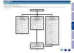
Page 74: ...MECHANICAL DISASSEMBLY Flowchart 1 FRONT PANEL ASSY 2 RADIATOR ASSY 3 BACK PANEL ASSY 4 TRANS EXPLODED VIEW PACKING VIEW Before Servicing This Unit Electrical Mechanical Repair Information Updating 74...

Page 75: ...VIEW M 11 RADIATOR ASSY DISASSEMBLY 2 RADIATOR ASSY and EXPLODED VIEW L AMP CONNECT PCB Ref No of EXPLODED VIEW B 02 3 R AMP CONNECT PCB Ref No of EXPLODED VIEW B 02 4 POSISTER1 2 PCB Ref No of EXPLOD...

Page 76: ...AVR X8500H E3 are used in this manual The viewpoint of each photograph Shooting direction X View from the top Shooting direction A Shooting direction B Shooting direction D Shooting direction C Front...

Page 77: ...H1L YELLOW SBL GRAY H3L ORANGE SL BROWN FL RED C BLUE R AMP CONNECT FR RED SR BROWN H3R ORENGE H1R YELLOW H2R PURPLE SBR GRAY N5833 N5834 N5842 N5841 PC SHEET Proceeding TOP COVER BACK PANEL ASSY 1 R...

Page 78: ...ROWN FL RED C BLUE R AMP CONNECT FR RED SR BROWN H3R ORENGE H1R YELLOW H2R PURPLE SBR GRAY N5833 N5834 N5842 N5841 PC SHEET x4 N6012 N6201 N9017 N9018 N9023 N9022 STYLE PIN Proceeding TOP COVER RADIAT...

Page 79: ...02 S16 S16 S01 S05 S03 S03 S03 S03 S03 S03 S08 S08 S03 S03 S03 S03 S03 S03 S03 S11 S03 S03 S03 S03 S03 S07 S07 S07 S02 S02 S02 S02 S02 S04 S04 S02 S17 S02 S17 S15 S15 S14 B02 3 B04 6 B05 3 B07 B01 B06...

Page 80: ...28 P29 P39 P07 P05 P03 P03 P43 P42 P06 P43 P42 P44 P45 P41 P09 P10 UK plug UK Only M87 AVR X8500H Parts List http dmedia dmglobal com Document DocumentDetails 24181 AVC X8500H Parts List http dmedia d...

Page 81: ...1 Version Display Mode 2 PANEL REMOTE LOCK Selection Mode 3 1 Selecting the Mode for Service related 3 2 Protection History Display Mode 3 3 232C Standby Clear Mode 3 4 Operation Info Mode 3 5 TUNER...

Page 82: ...y parts not fully connected into the connectors that connect the PCBs Is DC5V output even when the connector N6001 supplying power from the SMPS PCB to the DIGITAL PCB is removed Check the circuits ar...

Page 83: ...3708 C3320 Q3511 C3709 Q3513 Q3515 C3325 C3326 Q3517 C3327 C3710 C3328 R3301 C3711 R3302 C3712 R3303 C3713 R3304 C3714 C3715 R3305 C3716 R3306 C3717 R3307 C3718 R3308 C3719 Q3521 R3309 Q3523 Q3524 Q35...

Page 84: ...out R3746 Q3 Component Cr to Monitor out R3750 Q4 Component Y to DIGITAL PCB R3744 Q5 Component Cb to DIGITAL PCB R3748 Q6 Component Cr to DIGITAL PCB R3752 Q7 FFC connection error or contact failure...

Page 85: ...HDMI DVI cable Use a certified HDMI cable with the HDMI mark Replace the HDMI DVI cable with the one shorter than 5m 2m is recommended and check again Use an High speed HDMI cable with Ether net or Hi...

Page 86: ...ERR displayed Check the unit The TV is faulty Check the circuits around the IP SCALER U2800 DIGITAL PCB and DDR2 U3000 U3001 If there appear to be no problems U2800 or U3000 U3001 is faulty See HDMI...

Page 87: ...ECK 4 INPUT SURROUND MODE SOURCE Audio output OK HDMI Legacy PCM2ch or DolbyDigital or dts CHECK 6 INPUT Connect AVR s connected in HDMI audio out put OK HDMI This unit s HDMI OUT Other AVR s HDMI IN...

Page 88: ...the emitter resistor Replace the base resistor Replace the trimmer potentiometers NO NO NO NO NO NO YES Check the CPU 4 3 Analog audio No audio output Are the N9028 5 7pins in the A AUDIO VIDEO PCB re...

Page 89: ...LAN cable correctly inserted Insert the LAN cable correctly and then turn on the power again Check the connection environment Checking the unit YES YES YES Can the output voltage 5V to Q8007 FET SW b...

Page 90: ...y Is the antenna cable inserted correctly into Net work Module Is the Bluetooth device compatible with the A2DP profile Is the Bluetooth function enabled on the Blue tooth device Connect the antenna c...

Page 91: ...B is faulty Connect the connectors correctly 5 3 Cannot recognize the connected USB device YES NO NO NO Checking the unit If no picture is output YES Check the VIDEO circuit Are digital video signals...

Page 92: ...868 R215 R2869 C2891 R216 R3422 C2892 R217 R3423 C2893 R218 C2894 R219 R3425 C2895 U2801 C3641 C2896 U2802 R3427 C2897 C3450 R3428 C2898 C2899 C3453 R220 C3454 R3814 C3455 C3456 U103 C3457 R2877 R3817...

Page 93: ...503 R6538 0 R6535 OPEN 1SR154 D6526 D6527 1N4003 Z9000 SHIELD_CASE Z9001 RUBBER_FORM 3 1 2 1 2 3 4 4 10 8 7 3 1 11 6 5 V 1 X 2 C 3 F 4 S 5 D 7 2 12 1 2 1 2 Europe China OPEN 2 2 2 2M 2 2M A B C After...

Page 94: ...for deformed pins OK NG Check by following the flow chart for 3 Starting detecting the point of failure NOTE After checking troubleshooting 3 HDMI DVI check 3 Starting detecting the point of failure R...

Page 95: ...2 b Figure 1 Device Connection Method 2 Preparations for checking HDMI Switcher reception transmission register 2 3 Device configuration method PC settings Execute the serial communication program Te...

Page 96: ...exiting Setup Assistant execute the above Display changes Figure 4 Change of the Display of the Communication Start Button Name Press Figure 6 AVR settings All the indicator Lights Figure 6 FLD Displa...

Page 97: ...Error with HDMI SW1 U2401 MN864788 H1 03 Check item 14 Communication Error with HDMI SW2 U2601 MN864788 H1 05 Check item 25 Communication Error with VIDEO DECODER U2000 ADV7850 H1 06 Check item 17 Co...

Page 98: ...m the player played back on the TV correctly in each case ZONE2 OUT HDMI IN 1 4 Check item 4 Does a video signal come from HDMI OUT1 to TV correctly Turn Video Conversion OFF on the setup menu SETUP M...

Page 99: ...he PCB Recheck from check item 1 If it does not work replace the PCB Checking device U3401 MN864787 3 1 Error Code H1 01 failure detection procedure NO YES NO YES Go to next page YES Checking the rese...

Page 100: ...ion line Check HDMI SW U2601 or U2401 HDMI Tx U3401 and CPU U6201 patterns as well as soldering If there is no problem go to the next step Check the HDMI SW1 Remove the damping resistor R2460 R2461 of...

Page 101: ...sistor If there is still a problem the HDMI SW1 U2401 is faulty Replace with a new device The power supply circuit is faulty Replace the PCB Recheck from check item 1 If it does not work replace the P...

Page 102: ...Error Code H1 03 failure detection procedure NO YES NO YES Checking the reset waveform HDMI SW2 Check item 16 Checking the reset waveform Check the waveform Is the TP waveform of the TP near the HDMI...

Page 103: ...ailure detection procedure NO GUI U2800 is faulty Replace with a new device Recheck from check item 1 If it does not work replace the PCB The power supply circuit is faulty Replace the PCB NO YES YES...

Page 104: ...he I2C communication line again after replacing the FET Q2001 If there is still a problem the GUI U2800 is faulty Replace with a new device Check the I2C communication line GUI U2800 is faulty Replace...

Page 105: ...U3001 is defective Replace their IC Or replace the substrate 3 6 Error Code H1 15 failure detection procedure Checking device U2801 MX25L12835FMI 10G Check item 23 Write to the GUI ROM Recheck from ch...

Page 106: ...tween CPU U6201 and VIDEO DECODER U2000 If there is no problem the VIDEO DECODER U2000 is faulty Replace with a new device Recheck from check item 25 If it does not work replace the PCB NO Examples of...

Page 107: ...next page 3 8 Error Code H1 08 failure detection procedure NO DSP U102 is faulty Replace with a new device Recheck from check item 1 If it does not work replace the PCB The power supply circuit is fa...

Page 108: ...as well as soldering If there is no problem go to the next step Check the SPI communication line DSP1 DSP U102 is faulty Replace with a new device YES The diagram shows an example Signal patterns var...

Page 109: ...DSP2 Checking device U252 ADSP21573 Go to next page NO DSP U252 is faulty Replace with a new device Recheck from check item 1 If it does not work replace the PCB The power supply circuit is faulty Re...

Page 110: ...U6201 patterns as well as soldering If there is no problem go to the next step Check the SPI communication line DSP2 DSP U252 is faulty Replace with a new device YES The diagram shows an example Signa...

Page 111: ...communication line Check the CPU Is the waveform of the TP near the DIR U7004 correct like the one shown in the diagram when the power is turned on U7004 25pin CLK 23pin MISO 26pin CS 24pin MOSI Chec...

Page 112: ...ly circuit is faulty Replace the PCB Recheck from check item 1 If it does not work replace the PCB Checking device U3802 SiI9437 NO YES NO YES YES Checking the reset waveform ARC IC Check item 41 Chec...

Page 113: ...IN5 Is the return value C4 or C0 IN6 A2 or A0 IN7 91 or 90 Example i 002E 00FF 0001 C4 00 or 04 Detection of DDC is not OK 22 or 11 Detection of DDC is OK Go to check item 45 Go to check item 44 Go t...

Page 114: ...ce with a new device Recheck from check item 2 If it does not work replace the PCB HDMI Switcher1 U2401 is faulty Replace with a new device Check for a short circuit in the 5V line and the 5V Switch I...

Page 115: ...tcher1 U2401 from the HDMI input terminal If there is no problem the HDMI Switcher1 U2401 is faulty Replace with a new device HDMI Switcher1 U2401 is faulty Replace with a new device Recheck from chec...

Page 116: ...0 Checking the TMDS Check the TMDS waveform at the following test point N5010 HDMI OUT ZONE2 D2 D2 D1 D1 D0 D0 CK CK Check item 51 Check the communication Do CK and DA indicate 5V at the test point ne...

Page 117: ...e with a new device When the results of check item 48 are 31 or 21 or 11 or 01 Detection of HPD is OK Detection of RXSENSE is not OK When the results of check item 48 are 32 or 22 or 12 or 02 Detectio...

Page 118: ...esults of check item 48 are 30 or 20 or 10 or 00 Detection of HPD is not OK Detection of RXSENSE is not OK Check item 54 Checking the HPD and RXSENSE Does the test point near HDMI output terminal N501...

Page 119: ...r 80 IN2 44 or 40 IN3 22 or 20 IN4 11 or 10 Example i 0056 00FF 0001 88 00 or 04 Detection of DDC is not OK 22 or 11 Detection of DDC is OK Go to check item 58 Go to check item 57 Go to check item 59...

Page 120: ...er2 U2601 is faulty Replace with a new device Recheck from check item 3 If it does not work replace the PCB HDMI Switcher2 U2601 is faulty Replace with a new device Check for a short circuit in the 5V...

Page 121: ...lace with a new device Recheck from check item 3 If it does not work replace the PCB YES NO NO NO YES YES Check item 61 Check the TMDS CLK detection status of the register Send the following command f...

Page 122: ...turn it on again To check under the same conditions use the same procedure as that for checking Monitor 1 when checking the Monitor 2 output No video signal is output from both Monitor 1 and Monitor 2...

Page 123: ...HPD and RXSENSE register value of the HDMI Tx device Send the following command from Termite exe Send the command i 0000 0040 0001 Move to the branch destination according to the value returned Check...

Page 124: ...he following test point N3402 HDMI OUT MONITOR1 D2 D2 D1 D1 D0 D0 CK CK Check item 69 Check the communication Are the waveforms for CKL and DATA at the test point near the HDMI output connector N3402...

Page 125: ...ce with a new device When the results of check item 66 are 10 Detection of HPD is OK Detection of RXSENSE is not OK When the results of check item 66 are 20 Detection of HPD is not OK Detection of RXS...

Page 126: ...esults of check item 66 are 00 Detection of HPD is not OK Detection of RXSENSE is not OK Check item 72 Checking the HPD and RXSENSE Does the test point near HDMI output terminal N3402 indicate 3 3V Do...

Page 127: ...lowing items with the TV turned on Checking the HPD RXSENSE status register HDMI OUT2 Example i 0000 0040 0001 01 Detection of HPD is OK Detection of RXSENSE is not OK 03 Detection of HPD is OK Detect...

Page 128: ...or Are waveforms of DDCSCK and DDCSDA observed at the test point near the HDMI output terminal N3401 N3401 HDMI OUT MONITOR2 DDCSCK DDCSDA Checking the EDID register OUT2 HDMI Tx U3401 is faulty Repla...

Page 129: ...inal N3401 indicate Hi 3 5 V N3401 HDMI OUT MONITOR2 HPD Check the RXSENSE OUT2 Check the HPD OUT2 HDMI Tx U3401 is faulty Replace with a new device HDMI Tx U3401 is faulty Replace with a new device R...

Page 130: ...o the HDMI output terminal N3401 indicate Hi 3 5 V N3401 HDMI OUT MONITOR2 D2 D2 D1 D1 D0 D0 CK CK HPD Checking the HPD RXSENSE status register OUT2 HDMI Tx U3401 is faulty Replace with a new device R...

Page 131: ...branch destination according to the value returned Checking the 5V DDC status register HDMI DDC Buffer Example i 0006 00FF 0001 F8 78 or 70 Detection of 5V is not OK 00 or 04 Detection of DDC is not O...

Page 132: ...If it does not work replace the PCB Recheck from check item 4 If it does not work replace the PCB HDMI Tx U3401 is faulty Replace with a new device Check for a short circuit in the 5 V line the Front...

Page 133: ...s faulty Replace with a new device Example i 0006 00FF 0001 F8 YES YES NO NO Check item 86 Check the AUDIO signal output Check the AUDIO signal waveform at the following test point Is the waveform lik...

Page 134: ...rom the PLD Check the video signal waveform at the following test point Is the waveform like the sample U3401 61pin NO HDMI Tx U3401 is faulty Replace with a new device Check the peripheral pattern be...

Page 135: ...line HDMI Tx PLD Check the Video signal line PLD GUI NO NO Check the peripheral pattern between the HDMI Tx U3401 and PLD U3200 If there is no problem the HDMI Tx U3401 is faulty Replace with a new de...

Page 136: ...1 C3446 C9012 R2866 R2672 R213 C3447 C9013 R2867 R2673 R3420 C9014 R2868 R215 R2869 C2891 R216 R3422 C2892 R217 R3423 C2893 R218 C2894 R219 R3425 C2895 U2801 C3641 C2896 U2802 R3427 C2897 C3450 R3428...

Page 137: ...R8085 R1901 R8087 R8088 C3679 R6532 R253 C3487 R6533 R9220 X2000 U3200 C3488 R3460 R1909 R9221 R3461 C2101 C1931 R6535 R256 C1932 R3462 R3463 C1933 R9224 R3464 C2104 R8090 R259 R3465 R6539 C3682 R3466...

Page 138: ...only 3 6 Remote ID Setup Mode If there are multiple DENON AV receivers in the same area this mode prevents other AV receivers from being operated concur rently with this device See 3 6 Remote ID Setu...

Page 139: ...ther Mac Address Q3 WiFi Mac Address Q4 BT Mac Address Q5 Audyssey App Interface Version qModel destination information Serial Number L1 X8500H L2 SN Model name AVR AVC Region E3 E2 E1C JP wFirmware P...

Page 140: ...mory IP SCALER ERR 02 e GUI Serial Flash NG If the Main CPU version is not supported by the GUI Serial Flash ADV8003 is displayed as the first character of the GUI firmware version If GUI Serial Flash...

Page 141: ...XX XXXX X XX XX XX General Firmware Version GUI Image DTS Version Main A PLD GUI LEGO Version X 3 6 7 1 3 X X X X X X X 1 6 X X X X X X X 1 5 3 4 X 1 V PLD X X X 5 DSP2 X X X 4 DSP1 X X X 2 X X X 5 1...

Page 142: ...R f d button is pressed Press the ENTER button to set the currently displayed mode and restart the device The setting with is selected for each mode q L1 FP VOL LOCK On L2 FP LOCK On The buttons on th...

Page 143: ...the device q L1 1 SERVICE CHECK L2 2 PROTECTION Service Path Check Mode See DIAGNOSTIC MODE The Video and Audio paths can be checked This function is convenient for confirming problem paths in the pro...

Page 144: ...on in the abnormal state protection is activated after around 6 seconds and the power is turned off 3 DC if the last protection is DC L2 DC Cause DC output of the power amplifier is abnormal If the p...

Page 145: ...protection is being detected the POWER LED flashes in red to warn you depending on the protection status as follows 1 ASO DC protection Flashes at 0 5 second intervals 0 25 seconds lit 0 25 seconds un...

Page 146: ...TATUS button after starting up this device in Operation Info mode The following information is displayed in the following order 1 Accumulated operating time L1 Operation Time L2 Total ______H Time dis...

Page 147: ...STATUS simultaneously press the power button to turn on the power Select the 6 REMOTE ID using the CURSOR f d button then press the ENTER button to con firm 3 6 3 Operations 1 When Remote ID Setup mo...

Page 148: ...input sources The default factory setting is OFF 5 2 Starting up While holding down buttons BACK and CURSOR f simultaneously press the power button to turn on the power 5 3 Operations 1 The Additiona...

Page 149: ...he sequence number Previous logs on the USB flash drive are not overwritten The log is encrypted 8 2 Starting up While the power is on hold down buttons BACK and OPTION for at least 3 seconds 8 2 1 If...

Page 150: ...XD5 SSDA5 IRQ5 DS 110 PA3 RXD5 SSCL5 111 TRDATA3 PG7 112 PA2 RXD5 113 TRDATA2 PG6 114 PA1 SCK5 IRQ11 115 VCC 116 TRCLK PG5 117 VSS 118 PA0 119 TRSYNC PG4 120 P67 IRQ15 121 TRDATA1 PG3 122 P66 123 TRDA...

Page 151: ...E INPUT SELECTOR I2S SELECTOR I2S AK4490EQ x 8 PLD PCM9211PTR DIR INPUT ANALOG 2CH INPUT NETWORK INPUT DIGITAL INPUT HDMI INPUT HDMI FRONT ETHERNET Wifi USB OPTICAL COAXIAL A D_INPUT D A_OUTPUT ADC BL...

Page 152: ...1 5 Audio system confirmation items See the block diagram fig AXXth Paths to be confirmed Display Settings What to confirm 1 Analog fig A01 A01 ANALOG PASS Input Source CBL SAT Input Mode Analog fixed...

Page 153: ...utput Front L R b The input source can be switched to any source except CBL SAT 6 Analog AD MAIN ZONE fig A06a fig A06b A06 AD Input Source CBL SAT Input Mode Analog fixed Sound mode MULTI CH STEREO A...

Page 154: ...t Sp 6ch Dolby Sp None Height Layout Front Height Top Middle Rear Height MAIN ZONE On ZONE2 Off ZONE3 Off Analog input Speaker output S Back L R b The input source can be switched to any source except...

Page 155: ...EO Amp assign Custom Floor Layout 5ch SB Height Sp 6ch Dolby Sp None Height Layout Front Height Top Middle Rear Height Speaker Select Floor Height MAIN ZONE ON ZONE2 OFF ZONE3 OFF Setting Front Termin...

Page 156: ...standby mode make sure that the power supply of this unit is also put in the standby mode b The input source can be switched to any source except CBL SAT The ARC path can also be checked check this u...

Page 157: ...F02 FAN MID FAN CONT_LOW LOW FAN CONT_MID HIGH FAN CONT_HIGH LOW FAN CONT_MAX LOW MAIN ZONE ON ZONE2 OFF ZONE3 OFF Medium speed fan b The input source can be switched to any source except CBL SAT 3 Hi...

Page 158: ...SBR H2L H1L SR H2R H1R SL OUTE INH2 SBL INE SBR IND OUTE OUTB ING1 OUTC OUTF NJU72343 INA1 OUTB SW1 INA1 INB2 INC OUTD OUTH INB1 OUTA INB2 OUTC INE INH2 ING1 ING2 INF INA2 OUTA OUTF INF FR SW2 VOLUME...

Page 159: ...I2S_eARC DSD_eARC SPDIF_HDMIRX SPDIF_HDMIRX I2S DSD_eARC SPDIF_eARC SPDIF_eARC SPDIF_Z2HDMI SPDIF_HDMIRX I2S_NET I2S_NET PLLOUT Z3DAC_I2S Z3DAC_I2S Z2DAC_I2S Z2DAC_I2S Z2DAC_MUTE Z2DAC_MUTE Z3DAC_MUTE...

Page 160: ...SR H2R H1R SL OUTE INH2 SBL INE SBR IND OUTE OUTB ING1 OUTC OUTF NJU72343 INA1 OUTB SW1 INA1 INB2 INC OUTD OUTH INB1 OUTA INB2 OUTC INE INH2 ING1 ING2 INF INA2 OUTA OUTF INF FR SW2 VOLUME IC2 INC OUT...

Page 161: ...IN2 Cr_IN1 Cr_IN2 Cr_IN3 V_IN1 V_IN2 V_IN4 V_IN3 V_IN6 V_IN7 V_IN8 V_IN5 V_IN9 V_OUT3 Z2 V Select V_OUT2 Z1 V Select Cr_IN4 Cr_IN5 Cr_IN6 Cb_IN6 Cb_IN4 Cb_IN5 Y_IN6 Y_IN4 Y_IN5 TMDS TO D AUDIO SPDIF M...

Page 162: ...I2S_eARC DSD_eARC SPDIF_HDMIRX SPDIF_HDMIRX I2S DSD_eARC SPDIF_eARC SPDIF_eARC SPDIF_Z2HDMI SPDIF_HDMIRX I2S_NET I2S_NET PLLOUT Z3DAC_I2S Z3DAC_I2S Z2DAC_I2S Z2DAC_I2S Z2DAC_MUTE Z2DAC_MUTE Z3DAC_MUTE...

Page 163: ...SR H2R H1R SL OUTE INH2 SBL INE SBR IND OUTE OUTB ING1 OUTC OUTF NJU72343 INA1 OUTB SW1 INA1 INB2 INC OUTD OUTH INB1 OUTA INB2 OUTC INE INH2 ING1 ING2 INF INA2 OUTA OUTF INF FR SW2 VOLUME IC2 INC OUT...

Page 164: ...I2S_eARC DSD_eARC SPDIF_HDMIRX SPDIF_HDMIRX I2S DSD_eARC SPDIF_eARC SPDIF_eARC SPDIF_Z2HDMI SPDIF_HDMIRX I2S_NET I2S_NET PLLOUT Z3DAC_I2S Z3DAC_I2S Z2DAC_I2S Z2DAC_I2S Z2DAC_MUTE Z2DAC_MUTE Z3DAC_MUTE...

Page 165: ...SR H2R H1R SL OUTE INH2 SBL INE SBR IND OUTE OUTB ING1 OUTC OUTF NJU72343 INA1 OUTB SW1 INA1 INB2 INC OUTD OUTH INB1 OUTA INB2 OUTC INE INH2 ING1 ING2 INF INA2 OUTA OUTF INF FR SW2 VOLUME IC2 INC OUT...

Page 166: ...IN2 Cr_IN1 Cr_IN2 Cr_IN3 V_IN1 V_IN2 V_IN4 V_IN3 V_IN6 V_IN7 V_IN8 V_IN5 V_IN9 V_OUT3 Z2 V Select V_OUT2 Z1 V Select Cr_IN4 Cr_IN5 Cr_IN6 Cb_IN6 Cb_IN4 Cb_IN5 Y_IN6 Y_IN4 Y_IN5 TMDS TO D AUDIO SPDIF M...

Page 167: ...I2S_eARC DSD_eARC SPDIF_HDMIRX SPDIF_HDMIRX I2S DSD_eARC SPDIF_eARC SPDIF_eARC SPDIF_Z2HDMI SPDIF_HDMIRX I2S_NET I2S_NET PLLOUT Z3DAC_I2S Z3DAC_I2S Z2DAC_I2S Z2DAC_I2S Z2DAC_MUTE Z2DAC_MUTE Z3DAC_MUTE...

Page 168: ...SR H2R H1R SL OUTE INH2 SBL INE SBR IND OUTE OUTB ING1 OUTC OUTF NJU72343 INA1 OUTB SW1 INA1 INB2 INC OUTD OUTH INB1 OUTA INB2 OUTC INE INH2 ING1 ING2 INF INA2 OUTA OUTF INF FR SW2 VOLUME IC2 INC OUT...

Page 169: ...I2S_eARC DSD_eARC SPDIF_HDMIRX SPDIF_HDMIRX I2S DSD_eARC SPDIF_eARC SPDIF_eARC SPDIF_Z2HDMI SPDIF_HDMIRX I2S_NET I2S_NET PLLOUT Z3DAC_I2S Z3DAC_I2S Z2DAC_I2S Z2DAC_I2S Z2DAC_MUTE Z2DAC_MUTE Z3DAC_MUTE...

Page 170: ...SR H2R H1R SL OUTE INH2 SBL INE SBR IND OUTE OUTB ING1 OUTC OUTF NJU72343 INA1 OUTB SW1 INA1 INB2 INC OUTD OUTH INB1 OUTA INB2 OUTC INE INH2 ING1 ING2 INF INA2 OUTA OUTF INF FR SW2 VOLUME IC2 INC OUT...

Page 171: ...SR H2R H1R SL OUTE INH2 SBL INE SBR IND OUTE OUTB ING1 OUTC OUTF NJU72343 INA1 OUTB SW1 INA1 INB2 INC OUTD OUTH INB1 OUTA INB2 OUTC INE INH2 ING1 ING2 INF INA2 OUTA OUTF INF FR SW2 VOLUME IC2 INC OUT...

Page 172: ...SR H2R H1R SL OUTE INH2 SBL INE SBR IND OUTE OUTB ING1 OUTC OUTF NJU72343 INA1 OUTB SW1 INA1 INB2 INC OUTD OUTH INB1 OUTA INB2 OUTC INE INH2 ING1 ING2 INF INA2 OUTA OUTF INF FR SW2 VOLUME IC2 INC OUT...

Page 173: ...SR H2R H1R SL OUTE INH2 SBL INE SBR IND OUTE OUTB ING1 OUTC OUTF NJU72343 INA1 OUTB SW1 INA1 INB2 INC OUTD OUTH INB1 OUTA INB2 OUTC INE INH2 ING1 ING2 INF INA2 OUTA OUTF INF FR SW2 VOLUME IC2 INC OUT...

Page 174: ...I2S_eARC DSD_eARC SPDIF_HDMIRX SPDIF_HDMIRX I2S DSD_eARC SPDIF_eARC SPDIF_eARC SPDIF_Z2HDMI SPDIF_HDMIRX I2S_NET I2S_NET PLLOUT Z3DAC_I2S Z3DAC_I2S Z2DAC_I2S Z2DAC_I2S Z2DAC_MUTE Z2DAC_MUTE Z3DAC_MUTE...

Page 175: ...SR H2R H1R SL OUTE INH2 SBL INE SBR IND OUTE OUTB ING1 OUTC OUTF NJU72343 INA1 OUTB SW1 INA1 INB2 INC OUTD OUTH INB1 OUTA INB2 OUTC INE INH2 ING1 ING2 INF INA2 OUTA OUTF INF FR SW2 VOLUME IC2 INC OUT...

Page 176: ...I2S_eARC DSD_eARC SPDIF_HDMIRX SPDIF_HDMIRX I2S DSD_eARC SPDIF_eARC SPDIF_eARC SPDIF_Z2HDMI SPDIF_HDMIRX I2S_NET I2S_NET PLLOUT Z3DAC_I2S Z3DAC_I2S Z2DAC_I2S Z2DAC_I2S Z2DAC_MUTE Z2DAC_MUTE Z3DAC_MUTE...

Page 177: ...SR H2R H1R SL OUTE INH2 SBL INE SBR IND OUTE OUTB ING1 OUTC OUTF NJU72343 INA1 OUTB SW1 INA1 INB2 INC OUTD OUTH INB1 OUTA INB2 OUTC INE INH2 ING1 ING2 INF INA2 OUTA OUTF INF FR SW2 VOLUME IC2 INC OUT...

Page 178: ...I2S_eARC DSD_eARC SPDIF_HDMIRX SPDIF_HDMIRX I2S DSD_eARC SPDIF_eARC SPDIF_eARC SPDIF_Z2HDMI SPDIF_HDMIRX I2S_NET I2S_NET PLLOUT Z3DAC_I2S Z3DAC_I2S Z2DAC_I2S Z2DAC_I2S Z2DAC_MUTE Z2DAC_MUTE Z3DAC_MUTE...

Page 179: ...SR H2R H1R SL OUTE INH2 SBL INE SBR IND OUTE OUTB ING1 OUTC OUTF NJU72343 INA1 OUTB SW1 INA1 INB2 INC OUTD OUTH INB1 OUTA INB2 OUTC INE INH2 ING1 ING2 INF INA2 OUTA OUTF INF FR SW2 VOLUME IC2 INC OUT...

Page 180: ...SR H2R H1R SL OUTE INH2 SBL INE SBR IND OUTE OUTB ING1 OUTC OUTF NJU72343 INA1 OUTB SW1 INA1 INB2 INC OUTD OUTH INB1 OUTA INB2 OUTC INE INH2 ING1 ING2 INF INA2 OUTA OUTF INF FR SW2 VOLUME IC2 INC OUT...

Page 181: ...I2S_eARC DSD_eARC SPDIF_HDMIRX SPDIF_HDMIRX I2S DSD_eARC SPDIF_eARC SPDIF_eARC SPDIF_Z2HDMI SPDIF_HDMIRX I2S_NET I2S_NET PLLOUT Z3DAC_I2S Z3DAC_I2S Z2DAC_I2S Z2DAC_I2S Z2DAC_MUTE Z2DAC_MUTE Z3DAC_MUTE...

Page 182: ...SR H2R H1R SL OUTE INH2 SBL INE SBR IND OUTE OUTB ING1 OUTC OUTF NJU72343 INA1 OUTB SW1 INA1 INB2 INC OUTD OUTH INB1 OUTA INB2 OUTC INE INH2 ING1 ING2 INF INA2 OUTA OUTF INF FR SW2 VOLUME IC2 INC OUT...

Page 183: ...I2S_eARC DSD_eARC SPDIF_HDMIRX SPDIF_HDMIRX I2S DSD_eARC SPDIF_eARC SPDIF_eARC SPDIF_Z2HDMI SPDIF_HDMIRX I2S_NET I2S_NET PLLOUT Z3DAC_I2S Z3DAC_I2S Z2DAC_I2S Z2DAC_I2S Z2DAC_MUTE Z2DAC_MUTE Z3DAC_MUTE...

Page 184: ...SR H2R H1R SL OUTE INH2 SBL INE SBR IND OUTE OUTB ING1 OUTC OUTF NJU72343 INA1 OUTB SW1 INA1 INB2 INC OUTD OUTH INB1 OUTA INB2 OUTC INE INH2 ING1 ING2 INF INA2 OUTA OUTF INF FR SW2 VOLUME IC2 INC OUT...

Page 185: ...I2S_eARC DSD_eARC SPDIF_HDMIRX SPDIF_HDMIRX I2S DSD_eARC SPDIF_eARC SPDIF_eARC SPDIF_Z2HDMI SPDIF_HDMIRX I2S_NET I2S_NET PLLOUT Z3DAC_I2S Z3DAC_I2S Z2DAC_I2S Z2DAC_I2S Z2DAC_MUTE Z2DAC_MUTE Z3DAC_MUTE...

Page 186: ...SR H2R H1R SL OUTE INH2 SBL INE SBR IND OUTE OUTB ING1 OUTC OUTF NJU72343 INA1 OUTB SW1 INA1 INB2 INC OUTD OUTH INB1 OUTA INB2 OUTC INE INH2 ING1 ING2 INF INA2 OUTA OUTF INF FR SW2 VOLUME IC2 INC OUT...

Page 187: ...N2 Cr_IN1 Cr_IN2 Cr_IN3 V_IN1 V_IN2 V_IN4 V_IN3 V_IN6 V_IN7 V_IN8 V_IN5 V_IN9 V_OUT3 Z2 V Select V_OUT2 Z1 V Select Cr_IN4 Cr_IN5 Cr_IN6 Cb_IN6 Cb_IN4 Cb_IN5 Y_IN6 Y_IN4 Y_IN5 TMDS TO D AUDIO SPDIF MO...

Page 188: ...N2 Cr_IN1 Cr_IN2 Cr_IN3 V_IN1 V_IN2 V_IN4 V_IN3 V_IN6 V_IN7 V_IN8 V_IN5 V_IN9 V_OUT3 Z2 V Select V_OUT2 Z1 V Select Cr_IN4 Cr_IN5 Cr_IN6 Cb_IN6 Cb_IN4 Cb_IN5 Y_IN6 Y_IN4 Y_IN5 TMDS TO D AUDIO SPDIF MO...

Page 189: ...N2 Cr_IN1 Cr_IN2 Cr_IN3 V_IN1 V_IN2 V_IN4 V_IN3 V_IN6 V_IN7 V_IN8 V_IN5 V_IN9 V_OUT3 Z2 V Select V_OUT2 Z1 V Select Cr_IN4 Cr_IN5 Cr_IN6 Cb_IN6 Cb_IN4 Cb_IN5 Y_IN6 Y_IN4 Y_IN5 TMDS TO D AUDIO SPDIF MO...

Page 190: ...r_IN1 Cr_IN2 Cr_IN3 V_IN1 V_IN2 V_IN4 V_IN3 V_IN6 V_IN7 V_IN8 V_IN5 V_IN9 V_OUT3 Z2 V Select V_OUT2 Z1 V Select Cr_IN4 Cr_IN5 Cr_IN6 Cb_IN6 Cb_IN4 Cb_IN5 Y_IN6 Y_IN4 Y_IN5 TMDS TO D AUDIO SPDIF MONITO...

Page 191: ...IN2 Cr_IN1 Cr_IN2 Cr_IN3 V_IN1 V_IN2 V_IN4 V_IN3 V_IN6 V_IN7 V_IN8 V_IN5 V_IN9 V_OUT3 Z2 V Select V_OUT2 Z1 V Select Cr_IN4 Cr_IN5 Cr_IN6 Cb_IN6 Cb_IN4 Cb_IN5 Y_IN6 Y_IN4 Y_IN5 TMDS TO D AUDIO SPDIF M...

Page 192: ...I2S_eARC DSD_eARC SPDIF_HDMIRX SPDIF_HDMIRX I2S DSD_eARC SPDIF_eARC SPDIF_eARC SPDIF_Z2HDMI SPDIF_HDMIRX I2S_NET I2S_NET PLLOUT Z3DAC_I2S Z3DAC_I2S Z2DAC_I2S Z2DAC_I2S Z2DAC_MUTE Z2DAC_MUTE Z3DAC_MUTE...

Page 193: ...SR H2R H1R SL OUTE INH2 SBL INE SBR IND OUTE OUTB ING1 OUTC OUTF NJU72343 INA1 OUTB SW1 INA1 INB2 INC OUTD OUTH INB1 OUTA INB2 OUTC INE INH2 ING1 ING2 INF INA2 OUTA OUTF INF FR SW2 VOLUME IC2 INC OUT...

Page 194: ...IN2 Cr_IN1 Cr_IN2 Cr_IN3 V_IN1 V_IN2 V_IN4 V_IN3 V_IN6 V_IN7 V_IN8 V_IN5 V_IN9 V_OUT3 Z2 V Select V_OUT2 Z1 V Select Cr_IN4 Cr_IN5 Cr_IN6 Cb_IN6 Cb_IN4 Cb_IN5 Y_IN6 Y_IN4 Y_IN5 TMDS TO D AUDIO SPDIF M...

Page 195: ...I2S_eARC DSD_eARC SPDIF_HDMIRX SPDIF_HDMIRX I2S DSD_eARC SPDIF_eARC SPDIF_eARC SPDIF_Z2HDMI SPDIF_HDMIRX I2S_NET I2S_NET PLLOUT Z3DAC_I2S Z3DAC_I2S Z2DAC_I2S Z2DAC_I2S Z2DAC_MUTE Z2DAC_MUTE Z3DAC_MUTE...

Page 196: ...N2 Cr_IN1 Cr_IN2 Cr_IN3 V_IN1 V_IN2 V_IN4 V_IN3 V_IN6 V_IN7 V_IN8 V_IN5 V_IN9 V_OUT3 Z2 V Select V_OUT2 Z1 V Select Cr_IN4 Cr_IN5 Cr_IN6 Cb_IN6 Cb_IN4 Cb_IN5 Y_IN6 Y_IN4 Y_IN5 TMDS TO D AUDIO SPDIF MO...

Page 197: ...N2 Cr_IN1 Cr_IN2 Cr_IN3 V_IN1 V_IN2 V_IN4 V_IN3 V_IN6 V_IN7 V_IN8 V_IN5 V_IN9 V_OUT3 Z2 V Select V_OUT2 Z1 V Select Cr_IN4 Cr_IN5 Cr_IN6 Cb_IN6 Cb_IN4 Cb_IN5 Y_IN6 Y_IN4 Y_IN5 TMDS TO D AUDIO SPDIF MO...

Page 198: ...r PCB Shooting direction A x10 x1 x1 N6012 N9030 N6014 3 Remove the DIGITAL PCB from the chassis and turn it over Place an insulation sheet larger than the PCB underneath the DIGITAL PCB b Connect the...

Page 199: ...6pin V201 SURROUND BACK Rch N5823 3 4pin V201 HEIGHT1 Lch N5820 3 4pin V101 HEIGHT1 Rch N5844 4 5pin V101 HEIGHT2 Lch N5843 7 8pin V101 HEIGHT2 Rch N5823 1 2pin V101 HEIGHT3 Lch N5843 3 4pin V101 HEIG...

Page 200: ...with a USB flash drive 3 Update method when the DIGITAL PCB or network module is replaced Using a USB flash drive 4 Update Method for Service Region Settings 5 Normal Firmware Update Method from USB...

Page 201: ...3 R348 R6240 C2000 C7014 R349 C2001 R6242 C2002 C2003 R6243 R1230 C7018 R6244 C7019 R6245 Q2001 R6246 C2007 R6247 R351 R9511 R6249 R352 C316 R353 C123 C317 R9513 R354 C124 C318 R9514 R3754 R355 C319 C...

Page 202: ...able 1 Update download file when the DIGITAL PCB or network module is replaced Model Name Model Area Download from SDI AVR X8500H AVC X8500H ALL avr_40 prod update factory xxxx zip Table 2 Update down...

Page 203: ...ension cable when connecting the USB flash drive Save the update file on a blank USB flash drive for use If a USB flash drive cannot be updated replace it with a different USB flash drive and perform...

Page 204: ...hts red Display during USB update L1 Please wait L1 Updating L2 min L1 Update Completed It takes a maximum of approximately 25 minutes for update to complete 6 The unit restarts when update is complet...

Page 205: ...drive 4 2 Starting Service Region Settings NOTE Remove the LAN cable from this unit when updating Do not connect to a wired or wireless network We recommend a USB memory device that has an LED install...

Page 206: ...it for this unit to start up 3 Set the input source to HEOS Music Check that the display is as shown below L1 TuneIn Internet Radio or No Network Connection L2 HEOS Favorites L1 Content of the display...

Page 207: ...rmware No update required Latest version installed is displayed when the firmware version is up to date 4 OTA Update starts automatically The Standby LED lights red Display during OTA update L1 Please...

Page 208: ...e file 0006 Update file is corrupted Please check the file 000B Please contact customer service in your area b Check the power supply and communication lines of each device Device ID table Device ID Y...

Page 209: ...Copyright 2017 D M Holdings Inc All Rights Reserved www denon com...

Reviews: