


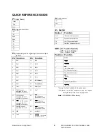


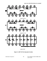


QUICK REFERENCE GUIDE
P1
(Input Power)
*+5vdc
*Gnd
-5vdc
P2
(Signal & Ref input)
*RH
*RL
Agnd
Agnd
*S1
*S3
*S4
*S2
P3
(Expansion port for digital input control & output
signals)
Pin Function
Pin Function
1
Bit 1
16
Bit 9
2
Bit 2
17
Bit 10
3
Bit 3
18
Bit 11
4
Bit 4
19
Bit 12
5
Bit 5
20
Bit 13
6
Bit 6
21
Bit 14
7 Bit
7
22 Bit 15 (Note 1)
8 Bit
8
23 Bit 16 (Note 1)
9
Gnd**
24
Built In Test
10
D0 (P3 control
requires SW1-6 off
and TB2-J7 in,J8 out)
25 Gnd**
11
D1 (P3 control
requires SW1-5 off
and TB2-J3 in,J4 out)
26
Inh
(P3 control
requires SW1-4 off)
12
Up
& Dn (P3 control
requires SW1-7 off
and TB2-J3 in,J4 out)
27
ENM
(P3 control
requires SW1-2 off)
13
Shift (P3 control
requires SW1-1 off)
28
ENL
(P3 control
requires SW1-8 off)
14 U/B
29 A
(LSB+1)
15 Cb/Z1
30
AquadB
(P3 control
requires SW1-3 off)
P4
(Test Points)
Vel
Gnd
E
S1, S2, S3
Socket Function
S1-A
*Resolver thin film/position
S1-B Synchro
thin
film/position
S2 LVDT
Component
Carrier
S3
Dual BW Component Carrier
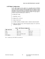
SW1 (10 Position Switch)
(Off = “Logic 1” Floating)
*(On = “Logic 0” Gnd)
Position Function
1 SHIFT
*2
ENM
3
AquadB
4
Inh
(Data Latch)
5
D1 (Resolution Control)
6
D0 (Resolution Control)
7
Up
/Dn
*8
ENL
9 Tp
(Factory
test
input)
10
EN
_
ZIP
*Factory Pre-Set Conditions & Required Inputs
**P3 pins 9 and 25 are common on card but require
both pins to be wired to the circuit ground.
Note 1: RD-19230EX-300 card only
Data Device Corporation
5
RD-19230EX-300 / RD-19240EX-300
User’s
Guide
Summary of Contents for RD-19230EX-300
Page 8: ......


