


PCI-DIO02 User’s Manual
9
4-2 J4 Connector (2Pin Header, 2.54mm)
This is a 3.3V external DC power connector. Power used when installing CPLD or FPGA, not
normally used.
4-3 JP1 Connector
JP1 is a JTAG (Joint Test Action Group) connector and is used to update the U1 CPLD
(XC95288XL) program of the board. Do not use when operating the board normally.
4-4 JP2 Connector
JP2 is a JTAG (Joint Test Action Group) connector and is used to update the FPGA program
on the board. Do not use when operating the board normally.
4-5 JP4 Connector
JP4 is a JTAG (Joint Test Action Group) connector and is used to update the U8 CPLD (XC9536)
program of the board. Do not use when operating the board normally.
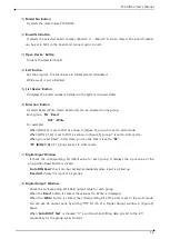
4-6
SW1
In a system that requires many I/O ports, if several DIO02 series boards are installed in one
system, each board address must be used separately. At this time, each board classification uses
the dip switch (SW1) on the board.
The total number of boards installed in one system is four.
SW1 Setup
2 1
ON
OFF
1
2
Board No.
OFF OFF
0
ON
OFF
1
OFF
ON
2
ON
ON
3
[Figure 4-2. Board Address Setup


