Dallas DS1821 Manual Download Page 12

DS1821 


12 of 18 

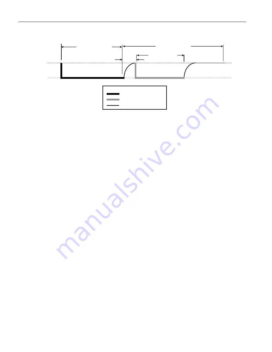
INITIALIZATION TIMING  

Figure 7 


READ/WRITE TIME SLOTS 

The bus master writes data to the DS1821 during write time slots and reads data from the DS1821 during 
read time slots.  One bit of data is transmitted over the 1-Wire bus per time slot. 
 

WRITE TIME SLOTS 

There are two types of write time slots: “Write 1” time slots and “Write 0” time slots.  The bus master 
uses a Write 1 time slot to write a logic 1 to the DS1821 and a Write 0 time slot to write a logic 0 to the 
DS1821.  All write time slots must be a minimum of 60 

μ

s in duration with a minimum of a 1 

μ

s recovery 

time between individual write slots.   Both types of write time slots are initiated by the master pulling the 
1-Wire bus low (see Figure 8). 
To generate a Write 1 time slot, after pulling the 1-Wire bus low, the bus master must release the 1-Wire 
bus within 15 

μ

s.  When the bus is released, the 5k pullup resistor will pull the bus high.  To generate a 

Write 0 time slot, after pulling the 1-Wire bus low, the bus master must continue to hold the bus low for 
the duration of the time slot (at least 60 

μ

s). 

The DS1821 samples the 1-Wire bus during a window that lasts from 15 

μ

s to 60 

μ

s after the master 

initiates the write time slot.  If the bus is high during the sampling window, a 1 is written to the DS1821.  
If the line is low, a 0 is written to the DS1821. 
 

READ TIME SLOTS 

The DS1821 can only transmit data to the master when the master issues read time slots.  Therefore, the 
master must generate read time slots immediately after issuing a read command (e.g., Read Temperature 
[AAh]), so that the DS1821 can provide the requested data.  All read time slots must be a minimum of 60 

μ

s in duration with a minimum of a 1 

μ

s recovery time between slots.  A read time slot is initiated by the 

master device pulling the 1-Wire bus low for a minimum of 1 

μ

s and then releasing the bus (see Figure 

8).   After the master initiates the read time slot, the DS1821 will begin transmitting a 1 or 0 on the bus. 
The DS1821 transmits a 1 by leaving the bus high and transmits a 0 by pulling the bus low.  When 
transmitting a 0, the DS1821 will release the bus by the end of the time slot, and the bus will be pulled 
back to its high idle state by the pullup resister.  Output data from the DS1821 is valid for 15 

μ

s after the 

falling edge that initiated the read time slot.  Therefore, the master must release the bus and then sample 
the bus state within 15 

μ

s from the start of the slot. 

LINE TYPE LEGEND 

Bus master pulling low 

DS1821 pulling low 

Resistor pull-up

V

DD


GND 

1-WIRE BUS 

480 

μ

s minimum 

480 

μ

s minimum

DS1821 T

X

presence pulse

60-240 

μ

MASTER T

X

 RESET PULSE

MASTER R

X

DS1821 

waits 15-60 

μ

Summary of Contents for DS1821

Page 1: ...ge NC No Connect DESCRIPTION The DS1821 can function as a standalone thermostat with user programmable trip points or as 8 bit temperature sensor with a 1 Wire digital interface The thermostat trip po...

Page 2: ...21 and pin descriptions are given in Table 1 The DS1821 can operate as a standalone thermostat with user programmable trip points or as 8 bit temperature sensor with a 1 Wire digital interface The ope...

Page 3: ...e and the counter is again preset with a starting value determined by the slope accumulator circuitry The preset counter value is unique for every temperature increment and compensates for the parabol...

Page 4: ...low thermostat trip point registers TH and TL and the configuration register and reading the temperature counter and slope accumulator registers Also in this mode the microprocessor can initiate and...

Page 5: ...URE DS1821 output temperature data is calibrated in degrees centigrade and is stored in two s complement format in the 1 byte 8 bit temperature register see Figure 3 which the user can access when the...

Page 6: ...ommand This value is the count remaining in the counter at the end of the gate period and is called COUNT_REMAIN in Eq 1 Next the Load Counter 41h command must be issued which loads the 9 bit slope ac...

Page 7: ...POL 0 Two bits in the status configuration register THF and TLF provide additional thermostatic information The value of these bits is normally 0 The THF temperature high flag bit will be set to 1 if...

Page 8: ...Read Write TLF 0 The measured temperature has not been lower than the value stored in the TL register TLF 1 At some point in time the measured temperature has been lower than the value stored in the...

Page 9: ...e to release the data line when the device is not transmitting data so that the bus is available for use by the other device The 1 Wire port of the DS1821 the DQ pin is open drain with an internal cir...

Page 10: ...versions will be performed until a Stop Convert T command is received STOP CONVERT T 22h Stops temperature conversions when the device is in continuous conversion mode 1SHOT 0 This opcode has no funct...

Page 11: ...ata from the counter register A0h Master receives 9 bit counter value from DS1821 Load Counter Loads slope accumulator data into the counter register 41h None 1 Wire SIGNALING The DS1821 uses a strict...

Page 12: ...high during the sampling window a 1 is written to the DS1821 If the line is low a 0 is written to the DS1821 READ TIME SLOTS The DS1821 can only transmit data to the master when the master issues read...

Page 13: ...OMMENDED MASTER READ 1 TIMING Figure 10 VDD GND 1 WIRE BUS 15 s VIH of Master TRC TINT 1 s Master samples VDD GND 1 WIRE BUS 15 s VIH of Master TRC small TINT small Master samples LINE TYPE LEGEND Fig...

Page 14: ...RX Presence DS1821 responds with presence pulse TX 02h Master issues Write TL command TX 0Ah Master sends data for TL 10 C TX Reset Master issues reset pulse RX Presence DS1821 responds with presence...

Page 15: ...mometer Error 55 C to 125 C VDD 3 6V to 5 5V See Typical Curve Figure 11 DQ Logic Low VIL 0 3 0 8 V 1 5 DQ Logic High VIH 2 The lower of 5 5 or VDD 0 3 V 1 6 Sink Current IL VDQ 0 4V VDD 3 6V to 5 5V...

Page 16: ...RSTH 480 s 1 Reset Time Low tRSTL 480 s 1 2 Presence Detect High tPDHIGH 15 60 s 1 Presence Detect Low tPDLOW 60 240 s 1 VDD Low to Mode Toggle Clock Low tPC 100 ns 1 3 Mode Toggle Clock 16 High to VD...

Page 17: ...DS1821 17 of 18 TYPICAL PERFORMANCE CURVE Figure 11 MODE TOGGLE TIMING WHEN T R 1 Figure 12...

Page 18: ...DS1821 18 of 18 TIMING DIAGRAMS Figure 13...

Reviews: