background image

SECTION 6.

VOLTAGE CHART

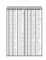
6-1. IC VOLTAGE (SP MODE)

1. IC151 (MC14053B)

PIN NO     

MODE

TV

LINE

1

0

0

2

0

3

4.8

4.8

4

4.9

4.9

5

4.9

4.9

6

0

0

7

0

0

8

0

0

43

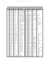
2. ICS01 (168K88E6ML)

PIN NO     

MODE

TV

LINE

1

2.3

2.3

2

2.3

2.3

3

4.9

4.9

4

0.2

0.2

5

0.1

0.1

6

4.1

4.1

7

4.9

4.9

8

2.6

2.6

9

3.0

3.0

10

2.6

2.6

PIN NO     

MODE

TV

LINE

11

0

0

12

0

0

13

0

0

14

0

0

15

0

0

16

2.3

2.3

17

2.3

2.3

18

0.3

0.3

19

0.3

0.3

20

4.9

4.9

PIN NO    

MODE

TV

LINE

9

0

12.0

10

0

12.0

11

0

12.0

12

4.9

4.9

13

4.9

4.9

14

4.9

4.9

15

0

0

16

12.0

12.0

All manuals and user guides at all-guides.com

all-guides.com

Summary of Contents for DV-F46N

Page 1: ...OO ELECTRONICS CO LTD Service Manual MODEL DV F46 26N DV F48 28N DV F54 34N DV F44 24N X POWER EJECT REC OTR CH TRACK REW FF PLAY STOP All manuals and user guides at all guides com a l l g u i d e s c...

Page 2: ...or more than 47K ohms 8 dBm unbalanced Output Audio line out Phono type connector less than 1K ohms 6dBm more than 47K ohms load unbalanced Frequency response 100 Hz 10KHz SP Signal to noise ratio Mor...

Page 3: ...nd locality 4 Leakage current test Confirm specified or lower leakage current between B earth ground power cord plug prongs and externally exposed accessible parts RF terminals antenna terminals video...

Page 4: ...POWER CIRCUIT SMPS 33 5 3 SYSCON CIRCUIT 35 5 4 LOGIC CIRCUIT 36 5 5 LOGIC CIRCUIT DV F54 F34N 37 5 6 PIF INPUT SELECTOR CIRCUIT 38 5 7 HEAD AMP CIRCUIT 39 5 8 VIDEO CIRCUIT 40 5 9 AUDIO CIRCUIT 41 5...

Page 5: ...CTION 1 CONTROLS AND FUNCTIONS 2 POWER EJECT REC OTR CH TRACK REW FF PLAY STOP POWER EJECT REC OTR REW FF PLAY STOP CH TRACKING FRONT DV F44 24N DV F46 26N All manuals and user guides at all guides co...

Page 6: ...3 CH REC REW FF STOP PLAY EJECT POWER PAUSE STILL STOP PLAY POWER CH CH EJECT REC OTR FRONT DV F48 28N DV F54 34N All manuals and user guides at all guides com a l l g u i d e s c o m...

Page 7: ...4 VIDEO AUDIO CH 3 CH 4 RF OUT ANT IN IN OUT REAR All manuals and user guides at all guides com...

Page 8: ...he rising edge of sw pulse Adjustment Inspection Standard 6 5 0 5 H SECTION 2 ELECTRICAL ADJUSTMENT Mode Adjustment Parts Check Point Test Equipments Test Tape Input Signal CH 1 PT01 PB R595 CH 2 VIDE...

Page 9: ...Adjust R395 to obtain 0 5 0 01 Vp p between the sync tip and 100 white level Adjustment Inspection Standard 0 5 0 01 Vp p 6 Mode Adjustment Parts Check Point Test Equipments Test Tape Input Signal LI...

Page 10: ...between the sync tip and 100 white level Adjustment Inspection Standard 2 0 0 2 Vp p 7 Mode Adjustment Parts Check Point Test Equipments Test Tape Input Signal CH 1 TJ313 PB 396 CH 2 VIDEO Oscilloscop...

Page 11: ...MHz component of multiburst signal becomes minimum Adjustment Inspection Standard Minumum 8 Mode Adjustment Parts Check Point Test Equipments Test Tape Input Signal LINE INPUT CH1 TJ313 Signal Gen ST...

Page 12: ...91 to obtain 3 33 0 1 MHz Adjustment Inspection Standard 3 33 0 1 MHz 9 Mode Adjustment Parts Check Point Test Equipments Test Tape Input Signal TJ391 STOP R391 GND Freq Counter Without signal Locatio...

Page 13: ...il Y recording current becomes minimum 6 Adjust R491 to obtain 80 5 mV Adjustment Inspection Standard 80 5 mV 10 Mode Adjustment Parts Check Point Test Equipments Test Tape Input Signal LINE INPUT CH1...

Page 14: ...obtain 300 10 mV at the position of SYNC Adjustment Inspection Standard 300 10 mV at the position of SYNC 11 Mode Adjustment Parts Check Point Test Equipments Test Tape Input Signal LINE INPUT CH1 TJ3...

Page 15: ...back frequency characteristics compared with 1KHz Recording playback output level 10KHz Recording playback output level is higher than the standard increase the record bias and if lower decrease it 12...

Page 16: ...ust connect GND into the primary GND But there is no connection when check the secondary circuit When change IC801 check FUSE and Cement resistance surely 13 Prepare the instrument connecting the insu...

Page 17: ...F802 normal Are R804 and D802 normal Is IC801 normal Change Change Change Change Is each voltage of secondary circuit normal Check the trans output of NO output stage Check the diode of NO output stag...

Page 18: ...f IC701 1 2 3 Is 5V at pin of IC701 7 Check X701 Check IC701 and change Check the Fuse of F802 Is 5V supplied to CATHOD of D712 Is 28V at D614 anode Check D814 and primary power circuit Change D614 Ch...

Page 19: ...65 67 69 It has not power failure compensation operation When disconnecting the power cord is 3 6V at pin and of IC601 26 81 Do pin and of IC601 oscillate 42 Is 5V applied to pin of IC601 37 Check IC...

Page 20: ...check the connection of CABLE Power On and select the VCR mode by pressing the TV VCR key YES YES YES YES NO NO NO D Set the TV channel to VCR 3 or 4 channel Check the Video Audio outputsignal of pin...

Page 21: ...S YES YES YES YES YES NO NO NO NO NO NO A Playback picture is not good Noise appears although adjusting tracking Is CTL pulse applied to pin of IC601 Noise shakes up and down on the screen Adjust trac...

Page 22: ...ayback Is Reel pulse applied to pin and of IC601 5 6 Check Flow A Is SW pulse supplied from pin of IC601 16 Check D PG input and connector Check pattern Check connector Head Amp and Head dust Change H...

Page 23: ...pin of P601 2 5V Is pin C PWM of IC601 Supplied Check connector and Motor 67 4 1 18 18 Check power circuit Check C505 R506 R507 and C516 Check IC601 Check power circuit Check circuit of R510 R511 R51...

Page 24: ...5V supplied Does X601 crystal oscillate Do S DATA CLK and RDY Signals of IC601 exchange with IC701 Is CAM SW DATA Correct Check IC602 Check IC 601 Check power circuit Check IC601 and X601 Check IC701...

Page 25: ...Is there the changes CAM DATA when CST IN Is 5V applied to pin of IC602 when CST IN 4 Chek IC602 Check connector Check DECK part Is 5V supplied at pin of IC601 Check PATTERN 45 Check IC601 H NO YES Y...

Page 26: ...IC201 Check Q204 and power circuit 7 Is 5V applied to pin of IC201 11 Is pin of IC201 0V 24 Is there Audio output pin of IC201 10 Is pin of IC201 GND 3 Check P601 and AC Head Check IC601 Check IC201...

Page 27: ...llate Check circuit adjacent to IC151 Check IC601 Check IC201 Is the voltage above 10V at pin of T201 Check Q201 collector above 10V Base 0V Check T201 Is record current 3 0mVrms Is pin of IC201 0V 1...

Page 28: ...601 pin Tuner mode H Line mode L Check PCB pattern Is 5V supplied to pin and of IC301 24 29 Check power circuit Check IC301 pin EE mode L PB mode H Check IC601 pin 29 Change IC301 Is signal input into...

Page 29: ...C301 Check IC301 pin EE mode L PB mode H Check Q301 Check QA02 QA03 Is composite video signal output from IC301 pin 11 1 2 6 Check power circuit Check IC601 pin Claen head or change head 29 24 4 29 NO...

Page 30: ...YES YES NO NO YES NO C REC VIDEO SIGNAL N G YES Check R399 R491 YES Is REC H Signal supplied at IC401 pin Check REC H Is REC singnal output from IC401 pin SP mode pin EP mode pin Is SW pulse input in...

Page 31: ...Check IC601 3 16 17 4 5 20 Is 5V supplied at ICS01 and pins 7 Is serial data input into ICS01 pin 3 4 5 Check oscillation of ICS01 16 17 Change ICS01 Check ON OFF 5V Check IC601 Check LS01 CS01 and C...

Page 32: ...All manuals and user guides at all guides com...

Page 33: ...All manuals and user guides at all guides com...

Page 34: ...All manuals and user guides at all guides com...

Page 35: ...All manuals and user guides at all guides com...

Page 36: ...All manuals and user guides at all guides com a l l g u i d e s c o m...

Page 37: ...All manuals and user guides at all guides com...

Page 38: ...All manuals and user guides at all guides com...

Page 39: ...All manuals and user guides at all guides com...

Page 40: ...All manuals and user guides at all guides com...

Page 41: ...All manuals and user guides at all guides com a l l g u i d e s c o m...

Page 42: ...All manuals and user guides at all guides com...

Page 43: ...All manuals and user guides at all guides com...

Page 44: ...All manuals and user guides at all guides com...

Page 45: ...All manuals and user guides at all guides com...

Page 46: ...E 1 2 3 2 3 2 2 3 2 3 3 4 9 4 9 4 0 2 0 2 5 0 1 0 1 6 4 1 4 1 7 4 9 4 9 8 2 6 2 6 9 3 0 3 0 10 2 6 2 6 PIN NO MODE TV LINE 11 0 0 12 0 0 13 0 0 14 0 0 15 0 0 16 2 3 2 3 17 2 3 2 3 18 0 3 0 3 19 0 3 0...

Page 47: ...0 5 11 23 6 12 0 5 13 0 14 20 1 15 20 1 16 20 1 17 20 18 23 2 19 23 2 20 0 21 0 PIN NO MODE REC 22 7 5 23 19 9 24 20 1 25 23 2 26 23 3 27 23 3 28 0 29 0 30 23 3 31 23 3 32 23 3 33 23 3 34 23 3 35 23...

Page 48: ...9 6 3 5 3 5 7 9 0 9 0 8 3 5 3 5 9 0 0 10 3 5 3 5 11 0 4 9 12 4 0 4 0 PIN NO MODE REC PB 13 3 2 3 2 14 0 0 15 4 1 4 1 16 4 1 4 1 17 0 0 18 4 1 4 1 19 4 1 4 1 20 0 0 21 4 1 4 1 22 4 1 4 1 23 0 0 24 4 9...

Page 49: ...4 12 2 4 2 4 13 2 0 2 0 14 3 0 3 0 15 2 4 2 4 16 2 2 2 2 17 3 7 3 7 18 2 3 2 3 PIN NO MODE REC PB 19 3 2 3 2 20 3 2 3 2 21 1 7 4 0 22 1 9 1 9 23 1 6 1 6 24 4 8 4 8 25 4 1 4 1 26 0 5 0 5 27 0 2 0 2 28...

Page 50: ...6 15 1 6 1 6 PIN NO MODE REC PB 16 0 0 17 3 9 0 18 0 0 6 19 0 0 20 4 1 0 21 4 1 0 22 0 0 6 23 0 0 24 0 0 25 0 0 26 0 0 27 0 0 28 0 0 29 0 0 30 0 0 PIN NO MODE REC PB 1 0 2 0 5 3 0 5 4 0 5 0 PIN NO MOD...

Page 51: ...13 CAP F R CAPSTAN FWD RVS L H 14 PB L PLAY LOW LOW 15 C ROTARY COLOR ROTARY PULSE 16 H A SWP HEAD AMP SWITCHING PULSE 17 ENVE COMP ENVELOPE COMPARE PULSE 18 V SWP VIDEO SWITCHING PULSE 19 Q Vsync Q V...

Page 52: ...CAP FG CAPSTAN FG INPUT PULSE 69 Vref OUT AMP REFERENCE Vcc 70 Vref In AMP REFERENCE Vcc 71 CLAMPF REFERENCE TO CTL CIRCUIT NO NAME ASSIGNMENT ACTIVE 72 CLAMPR REFERENCE TO CTL CIRCUIT 73 CTLAMPout R...

Page 53: ...9 Q315 2 4 0 1 7 Q316 1 6 0 3 0 0 2 3 0 Q317 3 8 0 5 0 5 0 4 5 0 Q402 1 6 0 6 0 0 0 9 0 Q403 1 7 4 9 2 3 Q405 0 0 1 0 5 3 VIDEO 4 VIDEO HEAD AMP PB mode REC mode PB mode REC mode Tr No Port Emitter C...

Page 54: ...6 17 18 19 20 21 22 23 24 25 26 27 28 29 30 31 32 33 34 35 36 37 38 39 40 41 42 43 44 45 46 47 48 49 50 51 52 53 54 55 56 57 58 59 60 61 62 63 64 65 66 67 68 69 70 71 72 73 74 75 76 77 78 79 80 81 82...

Page 55: ...ZN C BOTTOM FIX 6 PCB MAIN AS 1 7 97P0709100 BOARD ANT 1 HI PS 8 DECK TOTAL AS 1 9 97P2442100 BRKT TMIAS 1 10 7173401211 SCREW TAPPTITE 3 TT2 BIN 4x12 MFZN DECK AS FIX 11 7173401211 SCREW TAPPTITE 1 T...

Page 56: ...H PLATE 1 No Part Code Part Name Q ty Description Remark 1 97P0608400 CHASSIS MAIN 1 ABS HB 2 97PC146300 PANEL FRONT AS 1 3 PCB LOGIC AS 1 4 PCB MAINAS 1 5 97PB0348D DECK TOTAL AS 1 6 97P0455700 COVER...

Page 57: ...0 mm E 12 5 mm F 15 0 mm G 17 5 mm H 20 0 mm G 17 5 mm H 20 0 mm J 22 5 mm K 25 0 mm X Auto Insertion Z Auto Insertion Tolerance Symbol Tolerance F 1 G 2 J 5 K 10 M 20 N 30 Value Example 478 0 47 479...

Page 58: ...l Distance Code Voltage 0J 6 3V 1A 10V 1C 16V 1D 20V 1E 25V 1V 35V 1G 40V 1H 50V 1J 63V 2A 100V 2B 125V 2C 160V 2D 200V 2E 250V 2F 315V Characteristic Capacitance Temperature Coefficient ppm C Coeffic...

Page 59: ...100V 0 01MF J TAPPING C209 CEXE1H108A C ELECTRO 50V RS 0 1MF 5X11 TP REF PART CODE PART NAME PART DESCRIPTION C210 CMXM2A562J C MYLAR 100V 5600PF J TAPPING C211 CMXM2A103J C MYLAR 100V 0 01MF J TAPPI...

Page 60: ...2 C504 CEXF1H100A C ELECTRO 50V RSM 10MF 5X8 5 TP C505 CEXE1H100A C ELECTRO RS 50V 10MF 5X11 TP REF PART CODE PART NAME PART DESCRIPTION C506 CEXF1A470A C ELECTRO RSM 10V 47MF 6 3X7 C507 CEXF1A470A C...

Page 61: ...401 DZN4148 DIODE 1N4148 AUTO 52MM D405 DZN4148 DIODE 1N4148 AUTO 52MM D601 DZN4148 DIODE 1N4148 AUTO 52MM D602 DZN4003 DIODE IN4003 D603 DZN4003 DIODE IN4003 D604 DZZ5R6BM DIODE ZENER DZ 5 6BM AUTO D...

Page 62: ...01 4859242220 CONN WAFER YFW800 02 Q151 TZSR1004 TR KSR1004 AUTO Q152 TZTA1273Y TR KTA1273Y 966Y Q153 TZSR1004 TR KSR1004 AUTO Q154 TZTA1266Y TR KTA1266Y AUTO 1015Y REF PART CODE PART NAME PART DESCRI...

Page 63: ...3JCA R CHIP 1 10 15K OHM J 2012 R220 HRFT121JCA R CHIP 1 10 120 OHM J 2012 REF PART CODE PART NAME PART DESCRIPTION R221 HRFT331JCA R CHIP 1 10 330 OHM J 2012 R222 RD AZ243J R CARBON FILM 1 6 24K OHM...

Page 64: ...R505 HRFT273JCA R CHIP 1 10 27K OHM J 2012 R506 RD AZ103J R CARBON FILM 1 6 10K OHM J REF PART CODE PART NAME PART DESCRIPTION R507 HRFT472JCA R CHIP 1 10 4 7K OHM J 2012 R508 RD AZ182G R CARBON FILM...

Page 65: ...Z562J R CARBON FILM 1 4 5 6K OHM J R813 RD AZ221J R CARBON FILM 1 6 220 OHM J R814 RD AZ183J R CARBON FILM 1 6 18K OHM J R815 RD AZ103J R CARBON FILM 1 6 10K OHM J R816 RD AZ392J R CARBON FILM 1 6 3 9...

Page 66: ...ARBON FILM 1 6 100 OHM J R709 RD AZ101J R CARBON FILM 1 6 100 OHM J R710 RD AZ102J R CARBON FILM 1 6 1K OHM J R711 RD AZ103J R CARBON FILM 1 6 10K OHM J R712 RD AZ104J R CARBON FILM 1 6 100K OHM J R71...

Page 67: ...0J COIL PEAKING PL 10UH J TAPPING NPA01 97P6289620 CONN HOUSING 00 8370 071 000 800 PA01 97P6289590 CONN HOUSING 00 8370 041 000 800 PA02 4859241920 CONN WAFER YEAW025 08 REF PART CODE PART NAME PART...

Page 68: ...ODE PART NAME PART DESCRIPTION P703 97P8810714 CONN AS Y10714 2 0 7P 140MM P704 97P6291825 CONN HOUSING 00 8370 047 000 800 REF PART CODE PART NAME PART DESCRIPTION S751 5S10000002 SW JOG SHUTTLE SRGP...

Reviews: