background image

1. Safety Precautions

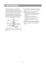
13.Outdoor Antenna Grounding - If an outside antenna is 

connected to the receiver be sure the antenna system is 
grounded so as to provide some protection against voltage 
surges and built-up static charges. Article 810 of the National 
Electrical Code, ANSI/NFPA 70, provides information with 
regard to proper grounding of the mast and supporting
structure, grounding of the lead-in wire to an antenna-dis
charge unit, size of grounding conductors,location of antenna-
discharge unit, connection to grounding electrodes and 
requirements for the grounding electrode.  See Figure 1.

14.Non-use Periods - The power cord of the appliance should be 

unplugged from the outlet when left unused for a long period 
of time.

15.Object and Liquid Entry - Care should be taken so that objects 

do not fall and liquids are not spilled into the enclosure through 
openings. 

16.Damage Requiring Service - The appliance should be 

serviced by qualified service personnel when:
  a) The power-supply cord or the plug has been damaged; or
  b) Objects have fallen, or liquid has been spilled into the
      appliance; or
  c) The appliance has been exposed to rain; or
  d) The appliance does not appear to operate normally or 
      exhibits a marked change in performance; or
  e) The appliance has been dropped, or the enclosure 
      damaged.

 17.Servicing - The user should not attempt to service the 

appliance beyond that described in the operating instructions. 
All other servicing should be referred to qualified service 
personnel.

ANTENNA DISCHARGE UNIT

(NEC SECTION 810-20)

ANTENNA LEAD

IN WIRE

POWER SERVICE GROUNDING

ELECTRODE SYSTEM

(NEC ART 250 PART H)

GROUND CLAMP

ELECTRIC

SERVICE

EQUIPMENT

GROUNDING CONDUCTORS

(NEC SECTION 810-21)

GROUND CLAMPS

EXAMPLE OF ANTENNA 

GROUNDING 

NEC - NATIONAL ELECTRICAL CODE

4

Summary of Contents for DV-135

Page 1: ...DV 135 Digital Home Cinema System ...

Page 2: ... IN COMPONENT OUTPUT Y OUTPUT DATA WAVEFORM IN COMPONENT OUTPUT 8 INTERNAL BLOCK DIAGRAM OF ICs 21 27 9 IC VOLTAGE CHART 28 29 10 BLOCK DIAGRAM 30 11 WIRING DIAGRAM 31 12 LEVEL DIAGRAM 32 13 SCHEMATIC DIAGRAM 33 41 FRONT SCHEMATIC DIAGRAM DSP SCHEMATIC DIAGRAM MPEG SCHEMATIC DIAGRAM MAIN SCHEMATIC DIAGRAM 1 POWER SCHEMATIC DIAGRAM 2 AMP SCHEMATIC DIAGRAM 3 INPUT SCHEMATIC DIAGRAM 4 VIDEO SCHEMATIC...

Page 3: ...ould be used only with a cart or stand that is recommended by th manufacturer 3 An appliance and cart combination should be moved with care Quick stops excessive force and uneven surfaces may cause the appliance and cart combination to overturn 4 Wall or Ceiling Mounting The appli ance should be mounted to a wall or ceiling only as recommended by the manufacturer 5 Ventilation The appliance should...

Page 4: ...that objects do not fall and liquids are not spilled into the enclosure through openings 16 Damage Requiring Service The appliance should be serviced by qualified service personnel when a The power supply cord or the plug has been damaged or b Objects have fallen or liquid has been spilled into the appliance or c The appliance has been exposed to rain or d The appliance does not appear to operate ...

Page 5: ...2 Specifications DV 135 5 ...

Page 6: ...utton 11 FM MODE button 12 MENU button 13 TONE button 14 SURROUND MODE button 15 MASTER VOLUME control 16 PHONES jack 17 PAUSE button 18 PLAY button 19 STOP button 20 Input selector VIDEO 1 VIDEO 2 TAPE MD TV buttons 21 Input selector DVD buttons 22 Input selector TUNER buttons 23 MOVE UP button 24 MOVE LEFT button 25 ENTER button 26 MOVE DOWN button 27 MOVE RIGHT button 28 ECHO LEVEL control Opti...

Page 7: ...ctors 13 FRONT SPEAKERS connectors 14 TV IN jacks 15 TAPE MD IN PLAY IN REC REC jacks 16 VIDEO 2 IN jacks 17 VIDEO 1 PLAY IN REC OUT jack 18 AC outlet Option Display 1 SURROUND MODE indicator 2 RDS indicator 3 PROGRAM indicator 4 STEREO indicator 5 DYNAMIC RANGE indicator 6 TUNED indicator 7 PBC Playback Control indicator 8 MEMORY indicator 9 MP3 indicator 10 PRESET indicator 11 REPEAT indicator 1...

Page 8: ...tton 17 GAME button 18 ZOOM button 19 DISPLAY button 20 D RANGE Dynamic Range button 21 FM MODE button 22 DIMMER button 23 TEST TONE button 24 REPEAT PTY button 25 RANDOM RDS button 26 TUNER PRESET buttons 27 CH LEVEL button 28 MOVE ENTER buttons 29 DELAY TIME button 30 TONE button 31 MEMORY button 32 TITLE button 33 PLAY MODE button 34 STOP button 35 OPEN CLOSE button 36 SKIP SEARCH DOWN button 3...

Page 9: ...4 Connecting to Equipment DV 135 Connecting to TV Scart Cable Optional 9 ...

Page 10: ...4 Connecting to Equipment DV 135 Connecting to AUDIO VIDEO 10 Remove the protective caps before making connections When not in use be sure to replace them ...

Page 11: ...ch Left ch Press and hold the lever Insert the stripped end of the cord Release the lever to replace it Right ch BLACK Left ch BLUE BLACK RED BLACK WHITE BLACK WHITE To prevent damage to circuits never short circuit the positive and negative speaker wires Do not connect the speaker cable to the L and R connectors at the same time and do not connect more than one speaker to the same speaker connect...

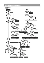
Page 12: ...gh Yes Check Protection circuit No No No No No No No 1 Does DVD appear at VFD Push power on Does loading appear at VFD Yes Does no DISC or time appear at VFD Yes Check if DVD an Audio Micom Interface is OK Yes Does Video1 2 MD TAPE TV FM 87 5kHz appear at VFD Yes OK Check from Micom to DVD Interface Check Power Check Loader Check MPEG PCB Yes Check Power Supply circuit No No No Does it not appear ...

Page 13: ...e FRONT POWER is OK Yes Check if the IC904 OSC PIN 40 waveform Yes Check if the IC904 PIN 44 45 is OK Check if POWER PART of the FRONT is OK Replace X901 Check if the VOLUME is OK Check if the HEADPHONE is OK Check if the REMOCON is OK Yes Yes Yes Yes Yes Check if the CN906 is OK Check if the FL901 PINS are OK Yes STANDBY ON No Yes Re connect it Refer to POWER SW PCB Refer to POWER SUPPLY circuit ...

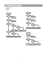
Page 14: ...ck SPEAKER system Refer to RELAY circuit Refer to MAIN AMP circuit STK402 050 No Yes Yes No No Check if the CN505 is OK Check if the IC510 PIN 3 4 waveform is OK Check if the CN502 PIN 7 waveform is OK Check if the IC712 PIN 6 waveform is OK Check if the IC508 PIN 20 waveform is OK Check if the IC518 PIN 3 waveform is OK Check if the IC521 PIN 14 waveform is OK Reconnect it Refer to DIR circuit IC...

Page 15: ...CS4228 No Yes MAIN VOLUME Abnormal Check if the M62446FP is OK Refer to FRONT PCB Refer to VOLUME IC M62446FP No Yes Optical in OK Refer to Dir circuit IC504 AK4112 Optional in Abnormal Check if the IC501 PIN 1 is OK Check if the IC501 PIN 3 is OK Refer to POWER SUPPLY circuit Yes Yes No No Check if the IC504 PIN 11 waveform is OK Check if the IC508 PIN 28 waveform is OK Replace OPTICAL IC Refer t...

Page 16: ...t Yes Yes No No No Yes OPEN CLOSE Abnormal Check if the FRONT CONTROL is OK Check if the CN706 is OK Check if the ATAPI Cable if is normally Check PN303 if is normally Check if the PN303 PIN 3 5 level is OK Check if the PN101A PIN 3 to 18 waveform is OK Replace MPEG PCB Check if the PN402 is OK Check PN101E if is normally Check POWER SUPPLY circuit Reconnect it Reconnect it Refer to FRONT PCB Reco...

Page 17: ...DVD Refer to IC102 MT1388 or replace DECK MECHA DVD Yes Yes Yes Yes Yes Yes Yes No No No No No No No DISC READ Abnormal Check if the CN706 is OK Check if the ATAPI Cable is normally Refer to PICK UP Unit or Replace DECK MECHA DVD Check POWER SUPPLY circuit Refer to IC302 BA5954FN or Replace DECK MECHA DVD Reconnect it Yes Yes No No Check if the IC302 PINS 1 26 is OK Refer to IC102 MT1388 Replace D...

Page 18: ...TECT THE UPDATE DISC LOAD LOADING DOOR CLOSE 3 READ THE DISC LOAD DOWNLOAD FROM CDROM 4 COMPLETED THE READ LOAD or NO DISPLAY DOWNLOAD FROM CDROM DOOR OPEN 1 5 COMPLETED THE UPDATE LOAD LOADING DOOR CLOSE DOOR CLOSE 6 SET THE KEY UNLOCK TUN PRESET OPEN DISAPPEAR LOCK MARK LOADING DOOR CLOSE 2 NOTE 2 AFTER COMPLETED POWER OUT AND IN AGAIN 1 AFTER DOOR OPEN EJECT THE UPDATE DISC CAUTION WHILE DOOR O...

Page 19: ......

Page 20: ......

Page 21: ...8 Internal Block Diagram of ICs DV 135 AK 4112A 21 ...

Page 22: ...8 Internal Block Diagram of ICs DV 135 AME1117 BU4052BCF ZR36710a 22 ...

Page 23: ...8 Internal Block Diagram of ICs DV 135 CS4228A ZR36701 23 ...

Page 24: ...e Control Serial Data SDATA AOUTA Analog Output A Serial Clock SCLK VA Analog Power ft Right Clock LRCK AGND Analog Ground Master Clock MCLK AOUTB Analog Output B SCL CCLK SCL CCLK REF_GND Reference Ground SDA CDIN SDA CDIN VQ Quiescent Voltage AD0 CS AD0 CS FILT Positive Voltage Reference CS4955 ES56033 24 ...

Page 25: ...8 Internal Block Diagram of ICs DV 135 CXP82852 25 ...

Page 26: ...Rin GNDS SWin AVSS AGND Lout Rout Cout SLout SRout RBASS1 RBASS2 RBASS3 RTRE CL2 CL1 CR2 CR1 SW out 21 20 19 18 17 15 14 13 12 11 10 9 8 7 6 5 4 3 2 1 42 41 40 39 38 37 36 35 34 33 32 31 30 29 28 27 26 25 24 23 22 tone tone volume volume volume volume volume volume MCU I F OUT PUT PORT 16 8 Internal Block Diagram of ICs DV 135 HY57V161610DTC 8 26 ...

Page 27: ...8 Internal Block Diagram of ICs DV 135 LA7952 NJM2068 NJU7313A 27 ...

Page 28: ...0 18 3 3 3 3 58 3 3 3 3 98 3 3 3 3 138 3 3 3 3 19 2 3 2 3 59 3 2 3 2 99 1 0 1 0 139 3 3 3 3 20 2 2 2 2 60 3 1 3 3 100 1 0 1 0 140 3 3 3 3 21 1 8 1 8 61 0 0 0 0 101 1 0 1 0 141 5 0 5 0 22 2 3 2 6 62 1 1 0 6 102 0 0 0 0 142 0 0 3 3 23 0 0 0 0 63 3 3 3 3 103 3 3 3 3 143 0 0 0 0 24 2 5 2 3 64 1 0 0 6 104 0 0 0 0 144 4 0 4 0 25 2 5 2 5 65 1 0 3 3 105 0 0 0 0 145 0 0 0 0 26 2 5 2 5 66 0 8 0 8 106 0 0 0 ...

Page 29: ...4 9 4 9 17 2 5 33 4 9 4 9 49 4 9 5 0 2 18 2 5 34 2 0 50 4 9 5 0 3 19 2 5 4 9 35 4 9 5 0 51 4 9 5 0 4 20 36 4 9 5 0 52 4 9 4 9 5 21 2 5 4 9 37 4 9 5 0 53 4 9 5 0 6 4 9 4 9 22 2 5 4 9 38 4 9 5 0 54 4 9 4 9 7 23 2 5 39 4 9 5 0 55 4 9 4 9 8 1 7 1 7 24 4 9 4 9 40 4 9 5 0 56 4 9 4 9 9 25 2 5 41 57 10 4 9 4 9 26 2 5 42 4 9 5 0 58 11 4 9 4 9 27 3 0 3 3 43 4 9 5 0 59 12 28 44 4 9 5 0 60 13 29 1 7 1 7 45 4 ...

Page 30: ...10 Block Diagram 30 DV 135 ...

Page 31: ...DV 135 11 Wiring Diagram 31 ...

Page 32: ... LEVEL Diagram 12 Level Diagram 32 DV 135 ...

Page 33: ...EUROPE RDS 50KHz 9KHz 50KHz 9KHz 100KHz 9KHz TUNER STEP FM AM 50KHz 9KHz 100KHz 9KHz 100KHz 10KHz FM BAND 87 5 108 87 5 108 87 5 108 522 1620 522 1620 530 1710 AM BAND 76 0 108 522 1620 10K 10K OPEN R987 6 8K 6 8K 2 4K 10K R988 10K 87 5 108 10K 2 4K 522 1620 87 5 108 OPEN 10K 522 1620 ...

Page 34: ...13 Schematic Diagram 34 DV 135 DSP 1 ...

Page 35: ...13 Schematic Diagram DV 135 DSP 2 35 ...

Page 36: ...13 Schematic Diagram DV 135 DSP 3 36 ...

Page 37: ...13 Schematic Diagram DV 135 MPEG 37 ...

Page 38: ... Main Schematic Diagram 1 Power Schematic Diagram 13 Schematic Diagram 38 ...

Page 39: ... Main Schematic Diagram 2 Amp Schematic Diagram 13 Schematic Diagram 39 ...

Page 40: ... Main Schematic Diagram 3 Input Schematic Diagram 13 Schematic Diagram 40 ...

Page 41: ... Main Schematic Diagram 4 Video Schematic Diagram 13 Schematic Diagram 41 ...

Page 42: ...1 2 BOTTOM View Front PCB 1 1 TOP View 14 Printed Circuit Diagram 42 DV 135 Front PCB ...

Page 43: ...2 BOTTOM View DSP PCB 1 TOP View 14 Printed Circuit Diagram 43 ...

Page 44: ...2 BOTTOM View MPEG PCB 1 TOP View 14 Printed Circuit Diagram 44 ...

Page 45: ...DV 135 MAIN PCB 14 Printed Circuit Diagram 45 ...

Page 46: ...2 BOTTOM View DV 135 MIC PCB 1 TOP View 14 Printed Circuit Diagram 46 ...

Page 47: ...15 Mechanism NO Q ty Description PART NAME Hexagon Ni Coated Ni Coated Ni Coated 47 DV 135 ...

Page 48: ...16 Exploded View and Mechanical Parts List 48 DV 135 ...

Page 49: ...9CD04122U0 SECC 0 8T SPRAY SILK 1 CE VERSION UL VERSION 32 COVER TOP 9CD0412100 SECC 0 7T SPRAY 1 33 SHIELD BOTTOM 9CD3303500 SECC T0 6 1 OPTION 34 SHIELD TOP 9CD3303600 SECC T0 6 1 OPTION NO PARTS NAME CODE NO DESCRIPTIONS Q TY REMARKS C1 FL DISPLAY DHNA11MM37 NHA 11MM37 1 C2 TRANS POWER 5TP8086851 5TP1086852 EI 85 8X63 230V 50Hz EI 85 8X63 127V 60Hz 1 CE VERSION UL VERSION C3 CORD AC 9736908600 ...

Page 50: ...16 Exploded View and Mechanical Parts List DV 135 50 ...

Page 51: ... CONN AS 22 P7 92 2P 460MM UL 1617 CN993 BACK M3 CP701 AC CORD 9728808100 WAFER GP390 03P TS M W O CENTER MAIN M4 CP705 CN701 REGURATOR 9728810500 CONN AS 24 P2 0 8P 140MM UL 1007 MAIN M5 CP710 CP852 VIDEO 9728810200 CONN AS 26 P2 0 6P 120MM UL 1007 MIC K1 CP907 CP711 MAIN 9728809500 CONN AS 26 P2 0 8P 200MM UL 1007 W KARAOKE MIC K2 CN905 CN504 DSP 9728811400 CONN AS P2 0 3P 270MM SHIELD BD W KARA...
Page 52: ... 75 C CHIP CERA C589 HCQK681JBA 50V CH 680PF J 1608 24 C ELECTRO C526 CEXF1E470E 25V RM 47MF 5X11 76 C ELECTRO C590 CEXF1H100E 50V RM 10MF 5X11 TP 25 C CHIP CERA C527 HCBK104KBA 50V X7R 0 1MF K 1608 77 C ELECTRO C591 CEXF1V470E 35V RM 47MF 5X11 TP 26 C ELECTRO C528 CEXF1E470E 25V RM 47MF 5X11 78 C ELECTRO C592 CEXF1H109E 50V RM 1MF 5X11 TP 27 C CHIP CERA C529 HCBK104KBA 50V X7R 0 1MF K 1608 79 C E...
Page 53: ...T103JBA 1 10 10K OHM J 1608 127 IC CHIP IC519 520 1NJM4558M NJM4558M 179 R CHIP R541 HRFT223JBA 1 10 22K OHM J 1608 128 IC IC521 1BU4052BCF BU4052 180 R CHIP R542L R HRFT151JBA 1 10 150 OHM J 1608 129 IC CHIP IC523 1NJM4558M NJM4558M 181 R CHIP R543L R HRFT103JBA 1 10 10K OHM J 1608 130 IC IC524 1M62446FP M62446FP 182 R CHIP R544L R HRFT472JBA 1 10 4 7K OHM J 1608 131 IC CHIP IC525 527 1NJM4558M N...

Page 54: ...CHIP D904 DZDS160 KDS160 230 R CHIP R599L R HRFT104JBA 1 10 100K OHM J 1608 33 DIODE D905 DZN4007 IN4007 231 R CHIP R600 HRFT474JBA 1 10 470K OHM J 1608 34 DIODE SW CHIP D906 DZDS160 KDS160 232 R CHIP R601 602 HRFT332JBA 1 10 3 3K OHM J 1608 35 DIODE ZENER D908 DZTZ6R8B MTZ6 8B 233 R CHIP R601A B C L R W HRFT101JBA 1 10 100 OHM J 1608 36 FL DISPLAY FL901 DHNA11MM37 NHA 11MM37 234 R CHIP R602A B C ...

Page 55: ...5SH1624368 EC16B241040B 37 C CERA C759A B C L R CCXF1H223Z 50V F 0 022MF Z TAPPING 86 RESONATOR CERA X901 5PCST10MTW CST10 00MTW 38 C CERA C760 CCXF1H223Z 50V F 0 022MF Z TAPPING 1 PCB H P AS 17000 9CDC0595B0 DV 135 39 C ELECTRO C761 CEXF1H100E 50V RM 10MF 5X11 TP 2 PCB H P B001 9CD6584501 242X329 40 C CERA C762 CCXF1H223Z 50V F 0 022MF Z TAPPING 3 C CHIP CERA C992 HCBK103KBA 50V X7R 0 01MF K 1608...

Page 56: ...B C L R RN01B100JS 1W 10 OHM J SMALL 91 DIODE ZENER D730 DZTZ5R6B UZ 5 6B 143 R CARBON FILM R726A B C L R RD AZ223J 1 6 22K OHM J 92 DIODE D731 741 DZN4148 1N4148 AUTO 52MM 144 R CARBON FILM R729 RD AZ153J 1 6 15K OHM J 93 DIODE D743 744 DZN4148 1N4148 AUTO 52MM 145 R METAL FILM R730 RN 4Z473J 1 4 47K OHM J 94 DIODE ZENER D745 DZTZ9R1B TZ 9 1V 146 R CARBON FILM R731 732 RD AZ473J 1 6 47K OHM J 95 ...

Page 57: ...C CHIP CERA C910 HCQK561JBA 50V CH 560PF J 1608 64 R CARBON FILM R921 RD 4Z331J 1 4 330 OHM J 13 C CHIP CERA C911 HCBK563KBA 50V X7R 0 056MF K 1608 65 R CHIP R923L R HRFT472JBA 1 10 4 7K OHM J 1608 14 C ELECTRO C912 CEXF1H100E 50V RM 10MF 5X11 TP 66 R CHIP R924L R HRFT103JBA 1 10 10K OHM J 1608 15 C CHIP CERA C913 HCBK392KBA 50V X7R 3900PF K 1608 67 R CHIP R925L R HRFT472JBA 1 10 4 7K OHM J 1608 1...

Page 58: ...HRFT102JBA 1 10 1K OHM J 1608 41 C CHIP CERA C479 HCQK221JBA 50V CH 220PF J 1608 93 R CHIP R431 HRFT220JBA 1 10W 22 OHM J 1608 42 C CHIP CERA C480 HCQK330JBA 50V CH 33PF J 1608 94 R CHIP R432 HRFT102JBA 1 10 1K OHM J 1608 43 C CHIP CERA C481 HCQK221JBA 50V CH 220PF J 1608 95 R CHIP R433 434 HRFT220JBA 1 10W 22 OHM J 1608 44 CLECTRO C482 CEXF1C221E RM 16V 220MF 6 3X11 TAT 96 R CHIP R435 436 HRFT820...

Page 59: ... Z TAPPING 9 CONN AS CP851 9728810300 26 P2 0 11P 220MM UL1007 10 CONN WAFER CP852 9728808600 2 0MM PH 6AW 6P 11 DIODE D851 855 DZN4148 1N4148 AUTO 52MM 12 IC SWITCH IC851 1LA7952 LA7952 13 JACK RCA JA851 9736323700 JE0200596N 14 JACK S VIDEO JA852 9736324000 C50160272N 15 JACK RCA JA853 9736323800 JE0301645N 16 JACK RCA JA854 9736323900 JE0301645G 17 TR Q851 852 TZTC3199Y KTC 3199Y TAPING 18 TR Q...

Reviews: