


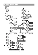


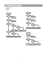


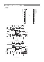
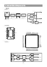
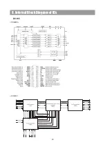


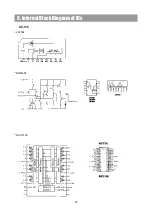
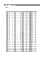

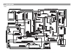


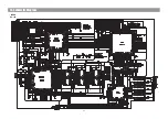


8. Internal Block Diagram of ICs
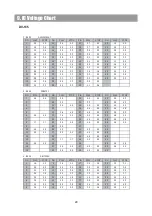
DV-135
CS434
C
O
15
2
14
3
13
4
16
1
11
6
10
7
9
8
12
5
Reset
RST
MUTEC
Mute Control
Serial Data
SDATA
AOUTA
Analog Output A
Serial Clock
SCLK
VA
Analog Power
ft/Right Clock
LRCK
AGND
Analog Ground
Master Clock
MCLK
AOUTB
Analog Output B
SCL/CCLK
SCL/CCLK
REF_GND Reference Ground
SDA/CDIN
SDA/CDIN
VQ
Quiescent Voltage
AD0/CS
AD0/CS
FILT+
Positive Voltage Reference
CS4955
ES56033
24
Summary of Contents for DV-135
Page 1: ...DV 135 Digital Home Cinema System ...
Page 5: ...2 Specifications DV 135 5 ...
Page 9: ...4 Connecting to Equipment DV 135 Connecting to TV Scart Cable Optional 9 ...
Page 19: ......
Page 20: ......
Page 21: ...8 Internal Block Diagram of ICs DV 135 AK 4112A 21 ...
Page 22: ...8 Internal Block Diagram of ICs DV 135 AME1117 BU4052BCF ZR36710a 22 ...
Page 23: ...8 Internal Block Diagram of ICs DV 135 CS4228A ZR36701 23 ...
Page 25: ...8 Internal Block Diagram of ICs DV 135 CXP82852 25 ...
Page 27: ...8 Internal Block Diagram of ICs DV 135 LA7952 NJM2068 NJU7313A 27 ...
Page 30: ...10 Block Diagram 30 DV 135 ...
Page 31: ...DV 135 11 Wiring Diagram 31 ...
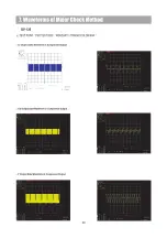
Page 32: ... LEVEL Diagram 12 Level Diagram 32 DV 135 ...
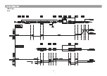
Page 34: ...13 Schematic Diagram 34 DV 135 DSP 1 ...
Page 35: ...13 Schematic Diagram DV 135 DSP 2 35 ...
Page 36: ...13 Schematic Diagram DV 135 DSP 3 36 ...
Page 37: ...13 Schematic Diagram DV 135 MPEG 37 ...
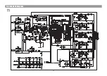
Page 38: ... Main Schematic Diagram 1 Power Schematic Diagram 13 Schematic Diagram 38 ...
Page 39: ... Main Schematic Diagram 2 Amp Schematic Diagram 13 Schematic Diagram 39 ...
Page 40: ... Main Schematic Diagram 3 Input Schematic Diagram 13 Schematic Diagram 40 ...
Page 41: ... Main Schematic Diagram 4 Video Schematic Diagram 13 Schematic Diagram 41 ...
Page 42: ...1 2 BOTTOM View Front PCB 1 1 TOP View 14 Printed Circuit Diagram 42 DV 135 Front PCB ...
Page 43: ...2 BOTTOM View DSP PCB 1 TOP View 14 Printed Circuit Diagram 43 ...
Page 44: ...2 BOTTOM View MPEG PCB 1 TOP View 14 Printed Circuit Diagram 44 ...
Page 45: ...DV 135 MAIN PCB 14 Printed Circuit Diagram 45 ...
Page 46: ...2 BOTTOM View DV 135 MIC PCB 1 TOP View 14 Printed Circuit Diagram 46 ...
Page 47: ...15 Mechanism NO Q ty Description PART NAME Hexagon Ni Coated Ni Coated Ni Coated 47 DV 135 ...
Page 48: ...16 Exploded View and Mechanical Parts List 48 DV 135 ...
Page 50: ...16 Exploded View and Mechanical Parts List DV 135 50 ...