15
CIRCUIT OPERATION MANUAL
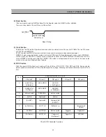
MemWait
Wait signal is produced in external device when accessing SRAM and peripheral devices. Wait signal is maintained as
Order status in the High status motivated by processor clock.
Not_OE
Read Strobe
ReadnotWrite
The ability to Read or Write of processing cycle.
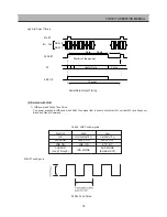
Access cycle of EMI Bank3 and Bank2 is as following feature. The value of timing chart can be modified by the value of
Configuration Register setting.
Symbol
Parameter
Min
Max
Units
Note
tCHAV
Referecne Clock high to Address valid
-8.0
0.0
ns
tCLSV
Reference Clock low to Strobe valid
-8.0
3.0
ns
tCHSV
Reference Clock high to Strobe Valid
-8.0
0.0
ns
tRCA/CH
Read Data valid to Reference Clock high
13.0
ns
tCHRDX
Read Data hold after Reference Clock high
-2.0
ns
tSVRDX
Read Data hold after Strobe valid
0.0
ns
1
tCLWOV
Reference Clock low to Write Data valid
-8.0
7.0
ns
1
tCHWOV
Reference Clock high to Write Data valid
-8.0
6.0
ns
1
tCHWDZ
Reference Clock high to Write data tristate
-8.0
6.0
ns
tCHRSV
Reference Clock high to remaining Strobes valid
-8.0
3.0
ns
tCHPH
Reference Clock high to ProcClkOut high
-8.0
0.0
ns
tWVCH
MemWait valid to Reference Clock high
13.0
ns
tRVCH
MemReq valid to Reference Clock high
13.0
ns
tRHWX
MemWait hold after ProcClkOut high
0.0
ns
1
tPHRX
Memreq hold after ProcClkOut high
0.0
ns
1
tPHEMIZ
MemGrant to signals tristate when bus granted
TBD
ns
1
Chart 4. EMI Timing Value
Summary of Contents for DSD-9255M
Page 17: ...16 CIRCUIT OPERATION MANUAL EMI Interface Timing...
Page 40: ...39 SCHEMATIC DIAGRAM...
Page 41: ...40 SCHEMATIC DIAGRAM...
Page 42: ...41 SCHEMATIC DIAGRAM...
Page 43: ...42 SCHEMATIC DIAGRAM...
Page 44: ...43 SCHEMATIC DIAGRAM...
Page 45: ...44 SCHEMATIC DIAGRAM...
Page 46: ...45 PARTS PLACEMENT ARRANGEMENT...
Page 47: ...46 PARTS PLACEMENT ARRANGEMENT...
Page 48: ...47 PARTS PLACEMENT ARRANGEMENT DSD 9255 FRONT DSD 9256 FRONT...
Page 49: ...48 PARTS PLACEMENT ARRANGEMENT...
Page 50: ...686 AHYEON DONG MAPO GU SEOUL KOREA C P O BOX 8003 SEOUL KOREA DAEWOO ELECTRONICS Corp...

