28
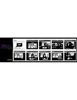
Troubleshooting charts
S1
Check the following signals.
HP : pin 6 of PW01V
5Vp-p
33.75KHz
VP : pin 7 of PW01V
5Vp-p
60Hz
Check HP signal of Q426’s base.
NO
Check HP signal is to pin 13 of IC216 through IC204.
Check IC204
Check VP signal is to pin 21 of IC212.
Check HP signal is to pin 14 of IC216 .
Check EVEN/ODD signal is to pin 1 of IC216.
Pins 9, 10, and 11 : High (to be HD Component ), Low (no HD Component)
Check IC209.
HP signal is input to pin 1. DEC_HS (HP) is output to pin 15.
EVEN/ODD (VP) signal is input to pin 13.
DEC_VS (EVEN/ODD) signal is output to pin 14.
Pins 9, 10, and 11 : High (to be HD Component ), Low (no HD Component)
Check EVEN/ODD signal is to pin 46 of IC 212
Check VP signal of Q415’s base.
NO
Check IC204.
YES
YES
YES
YES
YES
NO
NO
NO
Check IC212.
Check IC216.
YES
NO
Check IC209.
DEC_HS and DEC_VS of PA06D to DTV Decoder module
YES
END
Summary of Contents for DSC-30W60N
Page 60: ...59 10 1 Connection Diagram 10 Circuit Diagram...
Page 62: ...61 Circuit Diagram 10 3 Power Circuit...
Page 63: ...62 Circuit Diagram 10 4 Main Circuit...
Page 64: ...63 Circuit Diagram 10 5 Video1 Circuit...
Page 65: ...64 Circuit Diagram 10 6 Video2 Circuit...
Page 66: ...65 10 7 Audio Circuit Circuit Diagram...
Page 67: ...66 10 8 Com Filter Circuit Circuit Diagram...
Page 68: ...67 10 9 VM Circuit Circuit Diagram...
Page 69: ...68 10 10 Blanking Circuit Circuit Diagram...
Page 70: ...69 10 11 Jack A V CONTROL LED Circuit Circuit Diagram...
Page 71: ...70 10 12 CRT Circuit Circuit Diagram...
Page 72: ...71 11 Exploded View DSC 30W60N...
Page 73: ...72 Circuit Diagram 10 13...