background image


Kit Operation 

CY4502 EZ-

PD™ CCG2 Development Kit Guide, Doc. No. 001-96601 Rev. *G 

23 

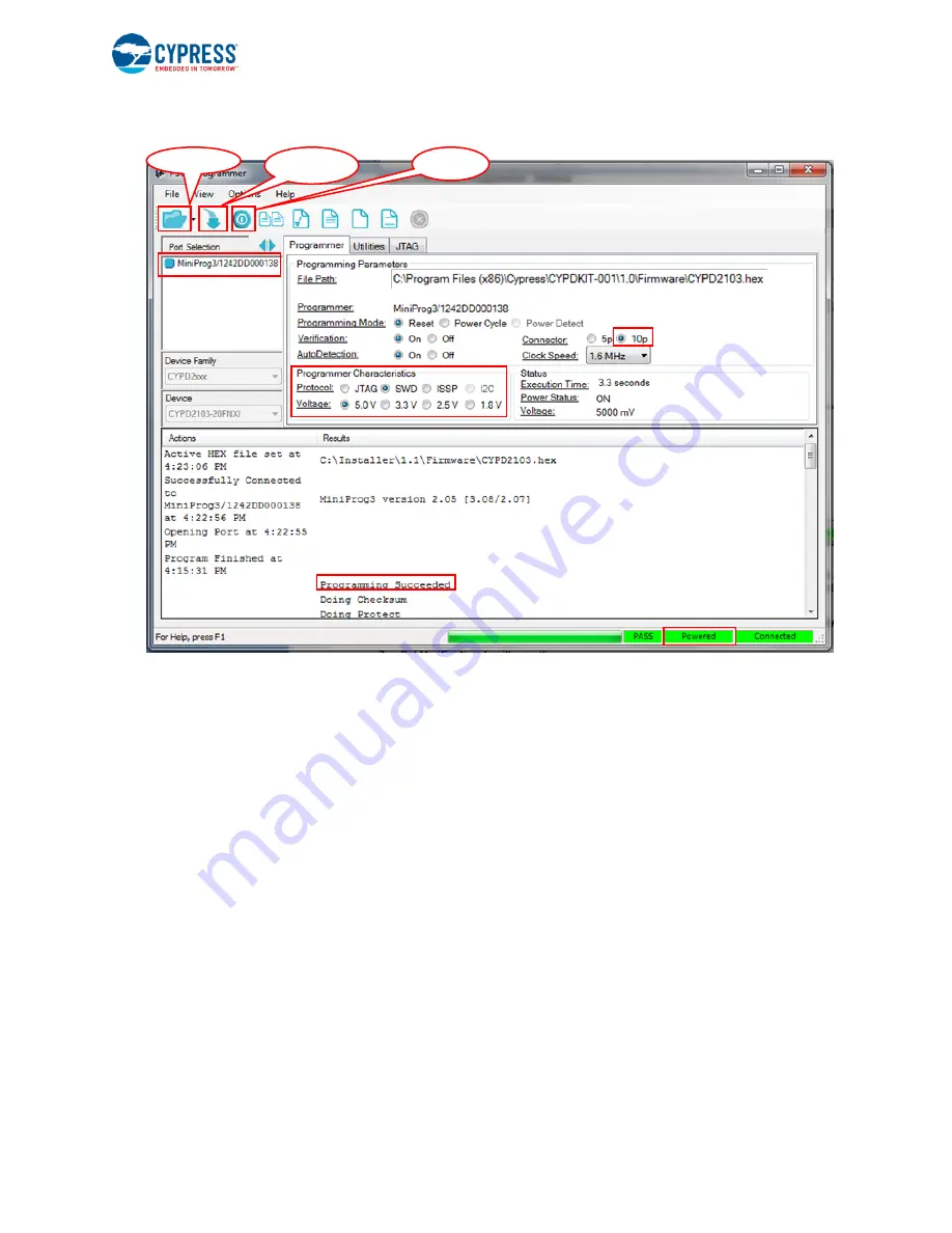
Figure 3-14. PSoC Programmer Window 


5.  Ensure that the settings on PSoC Programmer are as highlighted in Figure 3-14. 

6.  Click the 

File Load

 button and point to the appropriate hex file to load it. 

Note: 

Firmware images are not included as part of the CY4502 CCG2 DVK installer. The firmware image for the CSP 

(CYPD2103-20FNXIT)  and  the  DFN  (CYPD2103-14LHXIT)  parts  are  different.  Contact 

Cypress

  for  the  appropriate 

CCG2 firmware images. 

7.  The status message at the bottom right of the PSoC Programmer window will indicate if the board is powered or 

not. 

8.  If the board is not powered yet, click on the Power button and verify the status message as in step 7. 

9.  Use the Program button to program the hex file on to the chip. 

10.  When the file is successfully programmed, 

“Programming Succeeded” appears in the 

Actions

 window. 

3.8.2    Programming the CCG2 Device Using a CCG1 Host Board over the CC Line 

A  firmware  upgrade  application, 

EZ-PD  Configuration  Utility

,  is  provided  by  Cypress


and  can  be  downloaded  from 

www.cypress.com/ezpdutility

.  The  EZ-PD  Configuration  Utility  is  a  Microsoft Windows  Application,  which  can  be  used  to 

configure and program CCG2 devices in the USB Type-C cable directly over the CC line with the help of  the CCG1 Host 
and Client boards. This method can be deployed by cable manufacturers to provide upgrades to the user or to program the 
firmware  after  the  cable  assembly  is manufactured.  The  CCG2  device  allows  the firmware  of  the assembled  cable  to be 
upgraded over the CC line through a built-in bootloader.


File  Load 

Program  

Power  

Summary of Contents for EZ-PD CCG2 Development Kit

Page 1: ...CY4502 EZ PD CCG2 Development Kit Guide Doc No 001 96601 Rev G Cypress Semiconductor 198 Champion Court San Jose CA 95134 1709 Phone USA 1 800 858 1810 Phone Intnl 1 408 943 2600 http www cypress com...

Page 2: ...ted States and foreign United States copyright laws and international treaty provisions Cypress hereby grants to licensee a personal non exclusive non transferable license to copy use modify create de...

Page 3: ...all Software 11 3 Kit Operation 12 3 1 Theory of Operation 12 3 2 Jumpers 13 3 3 CCG2 Single Chip EMCA Application 14 3 4 CCG2 Two Chip EMCA Application One Chip Powered 16 3 5 CCG2 Two Chip EMCA Appl...

Page 4: ...ent Kit Guide Doc No 001 96601 Rev G 4 Appendix B PCB Layout 31 B 1 Top Layer 31 B 2 Bottom Layer 31 B 3 Ground Layer 1 32 B 4 Ground Layer 2 32 B 5 Power Layer 1 33 B 6 Power Layer 2 33 Revision Hist...

Page 5: ...station If an ESD workstation is not available use appropriate ESD protection by wearing an antistatic wrist strap attached to the chassis ground any unpainted metal surface on the board when handling...

Page 6: ...evelopment board provided with the DVK It documents different types of firmware downloading and debugging methods with detailed instructions This guide briefly explains the hardware interfaces availab...

Page 7: ...reference documentation Bracketed Bold Displays keyboard commands in procedures Enter or Ctrl C File Open Represents menu paths File Open NewProject Bold Displays commands menu paths and icon names i...

Page 8: ...lternate uses such as DisplayPort SCL I2 C serial clock line SDA I2 C serial data line SDK Software development kit Start of packet SOP K code marker used to delineate the start of a packet Three SOP...

Page 9: ...CY4502 CCG2 DVK page The installation package CY4502Setup exe contains the kit hardware files and documents Double click on CY4502Setup exe to start the installer Click Next on the first screen to sta...

Page 10: ...Wizard 3 Read and accept the license agreement for the software components and click Next The kit will now install on your machine Figure 2 3 Figure 2 3 Installation Progress 4 When installation is c...

Page 11: ...quired for this kit 2 3 Install Software When installing the CY4502 CCG2 DVK the installer checks if the required software is installed in the system If the required applications are not installed the...

Page 12: ...3 devices in the CY4502 board are shipped with factory programmed firmware that demonstrates the functionality of CCG2 controllers in EMCA USB PD Type C cables The CYPD2103 firmware implements a passi...

Page 13: ...the VDDD pins of U1 and U2 Note The configuration with both chips powered will work in this DVK irrespective of which Type C plug connector J1 or J2 is connected to the DFP Open Current measurement J...

Page 14: ...pers to enable SOP response of U2 CYPD2103 14LHXIT Short Enables SOP response by pulling GPIO D3 low The CYPD2103 firmware is configured to detect the presence of the VCONN supply in the VCONN1 VCONN2...

Page 15: ...L I2C_0 _SDA A3 A2 B4 CC1 GPIO GPIO D3 C2 CC2 A4 E4 VCONN1 C4 VCONN2 VDDIO E1 RD1 B3 VSS D4 GPIO D2 GPIO B2 GPIO C3 0 1uF 1uF VDDIO 4 7 k This EMCA solution contains CCG2 on only one of its plugs This...

Page 16: ...ation Diagram One Chip Powered VCONN1 VBUS CC Type C Plug Type C Plug VCONN2 GND SuperSpeed and HighSpeed Lines CCG2 CYPD2103 20FNXIT VDDD E3 A1 VCCD VSS C1 XRES B1 SWD_ IO SWD_ CLK E2 D1 I2C_0 _SCL I...

Page 17: ...pplication Both Chips Powered The CY4502 board can operate in the two chip EMCA application with both CCG2 controllers powered as shown in Figure 3 9 Follow these steps to configure the board for this...

Page 18: ...The same applies to the VCONN signal coming from the other end of the cable Both CCG2 devices will be powered one through VCONN1 and the other through VCONN2 VDDD The CCG2 powered through VCONN1 resp...

Page 19: ...controller U1 is powered J2 LED1 CCG2 controller U1 is powered CCG2 Two Chip EMCA Application one chip powered Section 3 4 J1 LED1 CCG2 controller U1 is powered J2 LED2 CCG2 controller U2 is powered C...

Page 20: ...Closed Provision for measuring current consumption on VCONN J11 Short 2 4 Board gets powered from mini USB connector J7 J12 Closed Provision for measuring current consumption of CCG1 Note Other jumpe...

Page 21: ...B flash can be programmed using the serial wire debug SWD interface or over the Type C Configuration channel CC signal 3 8 1 Programming the CCG2 Device Using PSoC Programmer and MiniProg3 A firmware...

Page 22: ...bug Kit from the Cypress webpage To use PSoC Programmer follow these steps 1 Start PSoC Programmer from Start All Programs Cypress PSoC Programmer 2 Connect one end of the USB cable to the MiniProg3 p...

Page 23: ...age as in step 7 9 Use the Program button to program the hex file on to the chip 10 When the file is successfully programmed Programming Succeeded appears in the Actions window 3 8 2 Programming the C...

Page 24: ...FP implementations can only initiate USB PD commands when a USB PD power contract is in place Since the DFP cannot setup a power contract while a power consumer Upstream Facing Port or UFP is not pres...

Page 25: ...nectors Headers Figure 4 1 CY4502 board Hardware Block Diagram SWD Connector for programming CCG2 LEDs CCG signal from USB Connector To Header CCG2 To Header Type C Plug Type C Plug SWD Connector for...

Page 26: ...per to select one chip two chip EMCA solution J8 J13 Jumpers to select the responsiveness to SOP packets for U1 U2 respectively J1 J2 USB Type C plugs J3 J4 SWD connectors J9 20 pin header Not mounted...

Page 27: ...ablish the signal orientation The other CC pin is repurposed as VCONN for powering the electronics in the USB Type C plug Also only one set of USB 2 0 D D wires is implemented in a USB Type C cable SB...

Page 28: ...cable plug power GND USB cable return current path Note Four capacitors are needed on the VBUS pins of the Type C connector according to the USB Type C specification A 10 nF bypass capacitor minimum...

Page 29: ...20 pin Header The CY4502 board contains one 20 pin header J9 that is not mounted on the DVK The CCG2 GPIOs and I 2 C lines are exposed on the 20 pin header Figure 4 7 The RD line from U1 VCONN and CC...

Page 30: ...ings are in accordance with those in CCG2 Two Chip EMCA Application both chips powered LED1 does not glow when connected in one chip two chip configuration Corrupted flash or blank flash of CCG2 contr...

Page 31: ...CY4502 EZ PD CCG2 Development Kit Guide Doc No 001 96601 Rev G 31 Appendix B PCB Layout B 1 Top Layer B 2 Bottom Layer...

Page 32: ...Appendix B PCB Layout CY4502 EZ PD CCG2 Development Kit Guide Doc No 001 96601 Rev G 32 B 3 Ground Layer 1 B 4 Ground Layer 2...

Page 33: ...Appendix B PCB Layout CY4502 EZ PD CCG2 Development Kit Guide Doc No 001 96601 Rev G 33 B 5 Power Layer 1 B 6 Power Layer 2...

Page 34: ...kit guide A 04 17 2015 GAYA Installer images and template updated B 04 21 2015 GAYA Updated How to Test the CY4502 Board C 05 06 2015 RRSH Updated Figure 3 13 D 05 29 2015 GAYA Removed PSOC programme...

Reviews: