


Quick Start
ADC1x13D series demonstration Board
Rev. 1.0 — April 2010
Quick Start
Document information
Info
Content
Keywords
JESD204A, CGV
TM
, Demonstration board, ADC, Labview
Abstract
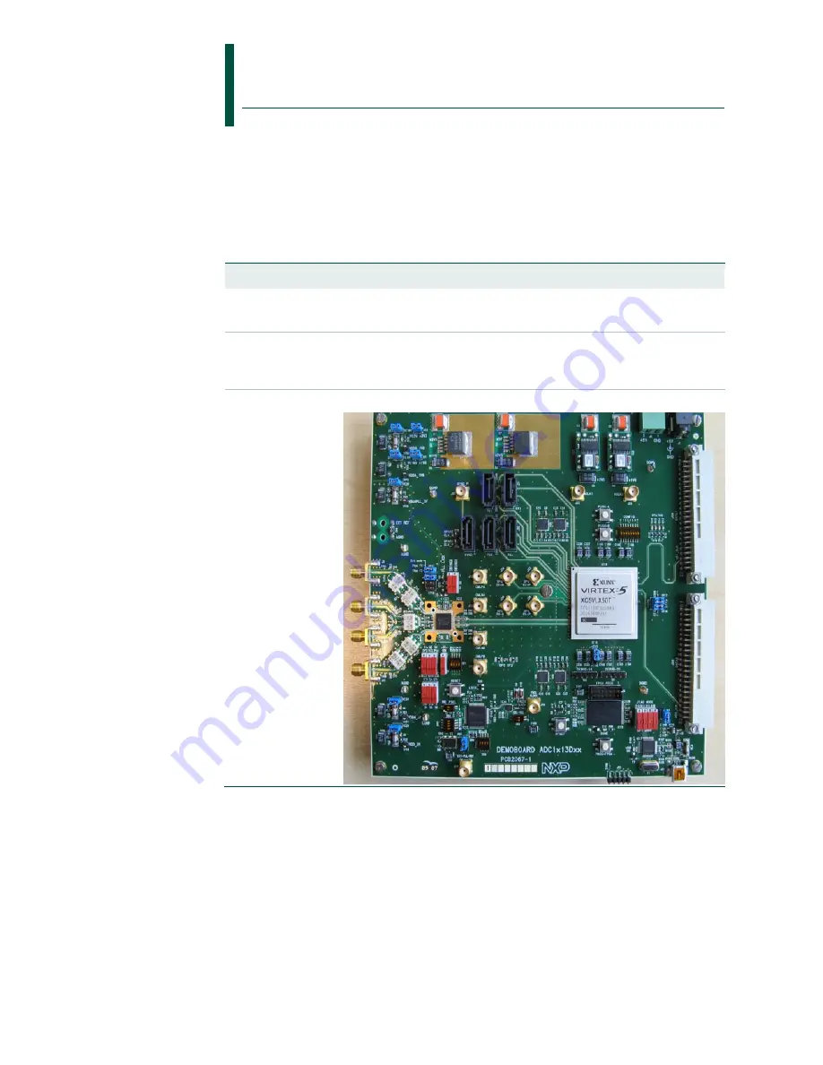
This document describes how to use the demonstration board for the
Analog-to-digital converter ADC1613D, ADC1413D, ADC1213D and
ADC1113D, JESD204A compliant.
Overview
Summary of Contents for ADC1 13D Series
Page 4: ......