


3.
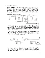
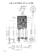
Receiver Circuit
In the receiver mode of operation, Q203 transistor is turned
off.
Also bias voltage is applied to Q103 and a proper b i a s a n d
AGC voltage is established to Q101, Q102, and Q103.
Q101 is a
27MHz RF input amplifier and any excessive input signal is
limited by diodes D101 and D102.
The amplified 27MHz is mixed
with VCO frequency selected by channel switch.
For channel 1
VCO is set at
16.27MHz.
The resulting first IF is 26.965 -
16.27 = 10.695MHz.
Q102,
is the first Converter,
and the
10.695MHz
is sharply filtered by L103 and a ceramic filter CFl.
The
first IF is again mixed with a second local oscillator of
10.24MHz.
10.695
-
10.24 « 0.455MHz.
Q103
is the second
Converter.
Second IF is
filtered by a razor sharp ceramic
filter of CF2 coupled with L104.
Q104
is a
first 455kHz
amplifier,
with Q105 being the last amplifier.
D103
is a
detector diode which produces audio signal as well as a negative
DC voltage for AGC action.
The negative voltage also provides
forward biasing to the cathode of ANL clipping diode of D106.
The biasing voltage has a time constance determined by RI24 and
C123.
Therefore,
any sharp negative going pulse from D103 will
back bias D106 and be clipped.
4.
Channel Up/Down Operation
The PLL
(TX/RX)
frequency,
channel number display, channel 9
select,
and PA/СВ mode select functions are controlled by a 4
bit microprocessor.
The Controls for channel sélection are the
Up and Down push buttons located on the front panel.
Depending
upon which button is pressed,
instructions are given to the
microprocessor to change the PLL frequency to the next channel.
If
the button
is
kept in the depressed position for
approximately 1.2
seconds the microprocessor will then scan
through the channels at a rate of approximately 5 channels per
second.
During channel
sélection or scan function,
inhibits the transmitter section of the
undesired signais from being radiated.
the microprocessor
unit,
to prevent
19 PLUS -4-
Summary of Contents for 19 Plus
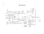
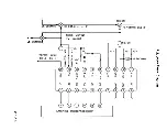
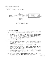
Page 7: ...19 PLUS 6 Block Diagram ...
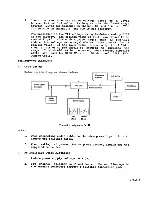
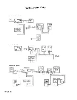
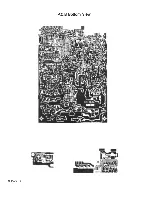
Page 8: ... z smd 61 T X 26 PLL Circuit Block Diagram ...
Page 15: ...ß CÛ 19 PLUS 14 ...
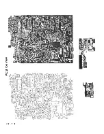
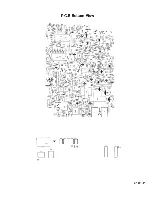
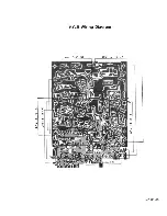
Page 17: ...P C B Bottom View 19 PLUS 16 ...
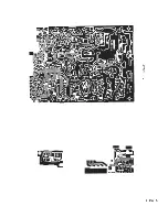
Page 18: ...401377 с 19 PLUS 17 40I06S ...
Page 25: ...Exploded View 19 PLUS 24 ...


