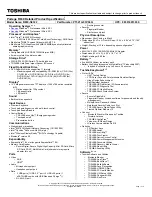
Schematic Diagrams
B - 4 Processor 2/7- CLK, MISC
B.Schematic Diagrams
Processor 2/7
PMSY S_PWRGD_BUF
H_PROCHOT#
H_CPUPWRGD_R
CAD Note: Capacitor need to be placed
close to buffer output pin
S3 circuit:- DRAM PWR GOOD logic
H_CPUPWRGD_R
R125
10K_04
Processor Pullups/Pull downs
TRACE WIDTH 10MIL, LENGTH <500MILS
BUF_CPU_RST#
H_PROCHOT#
R209
*39_04
R282
*0_04
C173
47p_50V_NPO_04
R213
75_04
R281
1K_04
R206
100K_04
R107
1K_04
R517
*10mil_short
R115
62_04
S
D
G
Q17B
MTDN7002ZHS6R
5
3
4
Q16
*MTN7002ZHS3
G
D
S
R211
*750_1%_04
R194
*200_04
S
D
G
Q17A
MTDN7002ZHS6R
2
6
1
R212
43.2_1%_04
R205
*1.5K_1%_04
R491
*0_04
Q14
MTN7002ZHS3
G
D
S
R116
56_1%_04
R193
*100K_04
R106
*0_04
R207
10K_04
R516
0_04
C707
0.047u_10V_X7R_04
R199
130_1%_04
R200
200_1%_04
CLO
CK
S
MI
S
C
TH
ER
MAL
PW
R MAN
AG
EME
NT
DDR
3
MIS
C
JTA
G &
B
PM
U36B
Iv y Bridge_rPGA_2DPC_Rev 0p61
SM_RCOMP[1]
A5
SM_RCOMP[2]
A4
SM_DRAMRST#
R8
SM_RCOMP[0]
AK1
BCLK#
A27
BCLK
A28
DPLL_REF_CLK#
A15
DPLL_REF_CLK
A16
CATERR#
AL33
PECI
AN33
PROCHOT#
AL32
THERMTRIP#
AN32
SM_DRAMPWROK
V8
RESET#
AR33
PRDY#
AP29
PREQ#
AP27
TCK
AR26
TMS
AR27
TRST#
AP30
TDI
AR28
TDO
AP26
DBR#
AL35
BPM#[0]
AT28
BPM#[1]
AR29
BPM#[2]
AR30
BPM#[3]
AT30
BPM#[4]
AP32
BPM#[5]
AR31
BPM#[6]
AT31
BPM#[7]
AR32
PM_SYNC
AM34
SKTOCC#
AN34
PROC_SELECT#
C26
UNCOREPWRGOOD
AP33
Q20
MTN7002ZHS3
G
D
S
R276
1K_04
R208
0_04
C315
68p_50V_NPO_04
C300
*0.
1u
_16V
_Y
5
V
_04
R496
*51_04
R275
4.99K_1%_04
U11
*MC74VHC1G08DFT1G
1
2
5
4
3
R148
100K_04
1.05VS_VTT
3.3VS
3.3V
1.5V
3.3V
1.5VS_CPU
3.3VS
1.05VS_VTT
1.05VS_VTT
CLK_EXP_N 19
CLK_EXP_P 19
CLK_DP_P 19
CLK_DP_N 19
H_PROCHOT#
40,42
H_THRMTRIP#
23
H_PECI
23,34
H_PM_SY NC
20
PLT_RST#
12,22,28
H_CPUPWRGD
23
DDR3_DRAMRST# 9,10
DRAMRST_CNTRL 6,19
H_SNB_IVB#
23
H_PROCHOT#_EC
34
SUSB
35,37,38
1.8VS_PWRGD
20,37
PM_DRAM_PWRGD
20
XDP_DBR_R
SM_RCOMP_2
SM_RCOMP_1
SM_RCOMP_0
H_PROCHOT#
H_PROCHOT#_D
XDP_TMS
XDP_TRST#
XDP_TCLK
VDDPWRGOOD_R
XDP_PREQ#
XDP_TDI_R
XDP_TDO_R
CPUDRAMRST#
DDR3 Compensation Signals
If PROCHOT# is not used,
then it must be terminated
with a 56-£[ +-5% pull-up
resistor to 1.05VS_VTT .
BUF_CPU_RST#
SM_RCOMP_1
SM_RCOMP_0
XDP_BPM1_R
XDP_BPM0_R
SM_RCOMP_2
XDP_BPM5_R
XDP_BPM4_R
XDP_BPM3_R
XDP_BPM2_R
PMSY S_PWRGD_BUF
XDP_PRDY #
XDP_BPM7_R
XDP_BPM6_R
Ivy Bridge Processor 2/7 ( CLK,MISC,JTAG )
Buffered reset to CPU
S3 circuit:- DRAM_RST# to memory
should be high during S3
CPUDRAMRST#
XDP_TDO_R
XDP_DBR_R
H_CATERR#
XDP_TRST#
XDP_TMS
H_SNB_IVB#
PU/PD for JTAG signals
XDP_PREQ#
XDP_TDI_R
XDP_TCLK
C301
*0.1u_10V_X5R_04
R183
140_1%_04
R521
200_1%_04
R520
25.5_1%_04
R493
*10mil_short
R499
51_04
R503
51_04
R494
51_04
R495
51_04
R498
51_04
CAD NOTE: All DDR_COMP signals
should be routed such that :-
- max length = 500 mils
- trace width = 15mils and
- MB trace impedance < 68 mohms
(worst case resistance)
CAD Note: Use pad sharing method
for following clock resistor placement
- CLK, MISC
Sheet 3 of 50
Processor 2/7-CLK,
MISC
Summary of Contents for W251ESQ
Page 1: ...W251ESQ W255ES ...
Page 2: ......
Page 3: ...Preface I Preface Notebook Computer W251ESQ W255ES Service Manual ...
Page 43: ...Top W251ESQ A 3 A Part Lists Top W251ESQ 灰色 尚盟 非耐落 Figure A 1 Top W251ESQ ...
Page 44: ...A 4 Top W255ES A Part Lists Top W255ES 灰色 尚盟 非耐落 Figure A 2 Top W255ES ...
Page 45: ...Bottom A 5 A Part Lists Bottom Figure A 3 Bottom ...
Page 46: ...A 6 SATA BLU RAY COMBO A Part Lists SATA BLU RAY COMBO 非耐落 志精 Figure A 4 SATA BLU RAY COMBO ...
Page 47: ...DVD DUAL A 7 A Part Lists DVD DUAL Figure A 5 DVD DUAL 非耐落 志精 ...
Page 48: ...A 8 LCD A Part Lists LCD 頭厚 非耐落 中性 Figure A 6 LCD ...
Page 49: ...LCD A 9 A Part Lists ...
Page 50: ...A 10 A Part Lists ...
Page 102: ...Schematic Diagrams B 52 B Schematic Diagrams ...