Schematic Diagrams
1V8_RUN/AON, NV3V3 B - 55
B.Schematic Diagrams
1V8_RUN/AON, NV3V3
1
1
2
2
3
3
4
4
5
5
6
6
7
7
8
8
A
A
B
B
C
C
D
D
C1
1V8_AON
2.6Amps @ 1.8V
1A
R1
D1
1A
DEFAULT SHORT
6-15-59381-7B0
R1
D1
C1
3A
3A
1V8_RUN
DEFAULT SHORT
6-15-59381-7B0
Rb
Rt
1.859V= 0.6 * (1+(20K/9.53K))
Open VREG Type 0
Vout= Vref * (1+(Rt/Rb))
3A
3A
Default
Default
NV3V3
1V8_AON
M:6-02-05841-CD0
S:6-02-08071-CD0
4/20
ආޣᖄԵ
2ND
DEFAULT SHORT
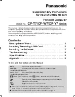
*1 VOUT rising time can be speed up if adding
R1 & D1 network between EN and GATE
*2 VOUT rising time can be slow down if adding
C1 between GATE and GND
*1 VOUT rising time can be speed up if adding
R1 & D1 network between EN and GATE
*2 VOUT rising time can be slow down if adding
C1 between GATE and GND
<NV_NET_MAX_CURRENT>
<MIN_LINE_WIDTH>
<NV_NET_MAX_CURRENT>
<MIN_LINE_WIDTH>
DGPU_PWR_EN_R
1V8_AON_PWRGD
NV3V3_EN
1.8V_RUN_EN
DGPU_PWR_EN_R
1.8V_RUN_EN
NV3V3_EN
VDD3
NV3V3
5V
VDD3
1V8_AON
1V8_RUN
5V
GND
GND
GND
GND
GND
GND
GND
3.3V
GND
3.3V
VDD3
1V8_AON
3.3V
5V
1V8_AON
NV3V3
12,13,14,27,55,63,64
1V8_RUN
14,15,24,25,28
1V8_AON
13,14,24,25,27,28,29,55,63,64,66
5V
32,43,45,46,50,52,53,55,57,59,60,61
VDD3
5,27,30,33,36,38,39,42,44,48,50,51,52,53,55,56,58,61,62,63,65,66
NV_1V8RUN_EN
29
NV_3V3_EN
29
NV_1V8AON_EN
29
3.3VS
3,9,10,11,12,13,29,30,32,33,34,35,36,38,39,40,41,42,44,48,49,50,51,52,59
3.3V
2,11,27,29,42,44,45,46,47,49,50,52,53,55,57,58
1V8_AON_PWRGD
29
Title
Size
Document Number
Rev
Date:
Sheet
of
6-71-P9500-D02A
D02A
[54] 1V8_RUN, 1V8_AON , NV3V3
A3
54
74
Tuesday, March 14, 2017
ᙔ!Ϻ!ႝ!တ!!DMFWP!DP/
P950HP
Title
Size
Document Number
Rev
Date:
Sheet
of
6-71-P9500-D02A
D02A
[54] 1V8_RUN, 1V8_AON , NV3V3
A3
54
74
Tuesday, March 14, 2017
ᙔ!Ϻ!ႝ!တ!!DMFWP!DP/
P950HP
Title
Size
Document Number
Rev
Date:
Sheet
of
6-71-P9500-D02A
D02A
[54] 1V8_RUN, 1V8_AON , NV3V3
A3
54
74
Tuesday, March 14, 2017
ᙔ!Ϻ!ႝ!တ!!DMFWP!DP/
P950HP
PR318
20K_1%_04
C730
10u_6.3V_X5R
_06
C289
10u_6.3V_X5R
_06
PC185
22u_6.3V_X5R
_08
C741
*0.1u_10V_X7R_04
PR88
*0402_short
PR409
10K_04
C290
*0
.1u_10V_X7R
_04
C731
10u_6.3V_X5R
_06
R103
100K_04
OpenVReg
PU12
EM5841BVT
DFN10
COMMON
1
FB
2
VCC
3
VIN
4
GND
5
GND
6
SW
7
SW
8
BOOT/NC
9
PGOOD
10
EN/FS
11
THERM
C713
10u_6.3V_X5R
_06
C288
10u_6.3V_X5R
_06
R108
10_06
D4
*RB0540S2
A
C
R523
*0402_short
R109
*10K_04
C687
100p_50V_NPO_04
S
D
G
Q11A
MTDK3S6R
2
6
1
R518
*10K_04
PR317
*20mil short-p
C738
*0.01u_10V_X7R_04
C688
1u_6.3V_X5R
_04
C677
*10u_6.3V_X5R
_06
R459
*10_06
PJ42
*1mm
1
2
PC187
22u_6.3V_X5R_08
U31
M5938BRD1U
EN
2
GATE
1
VIN
9
VOUT
8
VBIAS
4
GND
3
VOUT
7
VOUT
6
VOUT
5
S
D
G
Q43A
MTDK3S6R
2
6
1
PC186
22u_6.3V_X5R
_08
R110
*0402_short
PJ39
*3mm
1
2
S
D
G
Q43B
MTDK3S6R
5
3
4
C737
1u_6.3V_X5R
_04
PC191
3300p_50V_X7R_04
R506
100K_04
PR95
*160K_04
S
D
G
Q10B
MTDK3S6R
5
3
4
PU10
M5938BRD1U
EN
2
GATE
1
VIN
9
VOUT
8
VBIAS
4
GND
3
VOUT
7
VOUT
6
VOUT
5
D36
*RB0540S2
A
C
PC65
1u_6.3V_X5R_04
PR325
*10K_04
S
D
G
Q11B
MTDK3S6R
5
3
4
PR96
10K_1%_04
R511
10_06
R106
100K_04
PR326
10K_04
PR320
*20mil short-p
S
D
G
Q10A
MTDK3S6R
2
6
1
PJ36
*1mm
1
2
PR319
9.53K_1%_04
PC194
*0.22u_10V_X5R_04
PC66
0.1u_10V_X7R_04
PR73
10_06
PC197 *0.01u_16V_X7R_04
PL10
2.2uH_4*4*2.0
1
2
PJ41
*CV-40mil
1
2
PC189
0.1u_10V_X7R
_04
Sheet 54 of 74
1V8_RUN/AON,
NV3V3
Summary of Contents for P950HR
Page 1: ...P950HR ...
Page 2: ......
Page 3: ...Preface I Preface Notebook Computer P950HR Service Manual ...
Page 24: ...Introduction 1 12 1 Introduction ...
Page 42: ...Disassembly 2 18 2 Disassembly ...
Page 45: ...Top with FP A 3 A Part Lists Top with FP Figure A 1 Top with FP ...
Page 46: ...A 4 Top without FP A Part Lists Top without FP Figure A 2 Top without FP ...
Page 47: ...Bottom A 5 A Part Lists Bottom Figure A 3 Bottom ...
Page 48: ...A 6 Main Board A Part Lists Main Board Figure A 4 Main Board ...
Page 49: ...HDD A 7 A Part Lists HDD Figure A 5 HDD ...
Page 50: ...A 8 LCD A Part Lists LCD Figure A 6 LCD ...
Page 126: ...Schematic Diagrams B 76 B Schematic Diagrams ...