


- 3 -
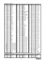
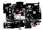
VRX630
10step wave
V
BB
V
BW
GND
VOLTS/DIV=0.1V(10:1PROVE)
A.B TIME/DIV=10usec.
Fig.1
1
2
3
4
5
6
7
8
9
10
0
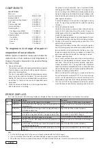
TROUBLESHOOTING
Problem
Nothing happens when
buttons are pressd.
Display is not accurate.
Cause
The microprocessor
has malfunction due to
noise,etc.
Measure
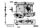
Turn off the power,then press the RELEASE lever
and remove the DCP.Press the Reset button for about
2 seconds with a thin rod.
Reset button
CLOCK ADJUSTMENT
1. Press the ADJ button to display the adjustment selec-
tion display.
2. Move the JOYSTICK up or down to select CLOCK,then
press ENT at the center of the JOYSTICK to display the
clock adjustment display.
3. Move the JOYSTICK left or right to select HR or MIN,then
move the JOYSTICK up or down to adjust the time.
※
The time is displayed in 12-hour format.
4. Pressing ENT at the center of the JOYSTICK when the
cursor is above HR or MIN saves the adjusted value in
memory and simultaneously returns the display to the
previous display(adjustment selection display).
To cancel clock adjustment before completion,use the
JOYSTICK to move the cursor to MENU,then press ENT
at the center of the JOYSTICK.
ADJUSTMENTS
Dot clock adjustment(at Digital PWB)
1. Turn the screen on,and connect TP601(TEST) to GND.
2. Adjust TC601 so that the reading of the frequency counter
at TP602(VSYNC) is 12.00MHz+0.01/-0.02MHz.
DC-DC converter output voltage adjustment
(at LCD PWB)
1. Adjust VR701 so that the voltage of TP703 is 5.05+0.05/
-0.052V.
2. Make sure the voltage has become the following value
at each test point.
TP702 : 7.5+0.5/-0.5V
TP704 : 18.5+1.0/-1.0V
TP701 : -15.5+1.0/-1.0V
Frequency of IC706 adjustment(at LCD PWB)
1. Adjust VR708 so that the frequency of TP712 is 144kHz.
VIDEO signal adjustment(at LCD PWB)
Input the visual signal(10step wave,monochrome,APL=50%,
1.0Vp-p)to the VIDEO input.
1. BRIGHT voltage confirmation(NTSC mode)
Make sure the voltage of TP706 is 1.88+0.1/-0.1V.
2. RGB-AMP/CONT-G adjustment(NTSC mode)
Adjust VR707(RBG AMP) so that VBB voltage of TP710
is 4.0+0.5/-0.5V.
Adjust VR703(CONT) so that VBW voltage of TP710 is
3.8+0.05/-0.05V.
3. BRT-R Adjustment(NTSC mode)
Adjust VR705(BRT-R) so that VBB voltage of TP711 is
4.0+0.05/-0.05V.
4. BRT-B Adjustment(NTSC mode)
Adjust VR706(BRT-B) so that VBB voltage of TP709 is
4.0+0.05/-0.05V.
5. COM-AMP adjustment(NTSC mode)
Adjust VR704(COM-AMP) so that the amplitude of TP705
is 6.7+0.1/-0.1Vp-p.
6. Burst cleaning adjustment(PAL mode)
Input a color ber signal.
Adjust L709 so that the wave form of TP709 is in focus.
VCOM DC bias adjustment
Adjust VR702(VCOM DC) to obtain the optimum contrast.
Burst cleaning
Fig.2
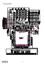
EXPLANATION OF IC
M30624MGA-173GP 052-6043-40
AV Center System Controller (Tuner, LCD panel, Ce-NET)
1.Terminal Description
pin 1 : LCD COLOR
: O : Color control signal output to LCD panel.
pin 2 : LCD HUE
: O : Hue control signal output to LCD panel.
pin 3 : IR IN
: IN : Signal input from Remote controller.
pin 4 : AMP REM OUT : O : Amplifier ON signal output terminal.
pin 5 : NU
: IN : Not in use.
pin 6 : BYTE
: IN : Connect to ground.
pin 7 : CNVSS
: IN : Connect to ground.
pin 8 : SUB CLCK I
: IN : Crystal connection for sub clock.
pin 9 : SUB CLCK O
: O : Crystal connection for sub clock.
pin 10: RESET_
: IN : Reset signal input. Negative logic.
pin 11: X OUT
: O : Crystal connection for main clock (10MHz).
pin 12: VSS
: - : Ground.
pin 13: X IN
: IN : Crystal connection for main clock (10MHz).
pin 14: VCC
: - : Positive supply voltage.
pin 15: NMI
: IN : Not in use.
pin 16: ACC DET
: IN : ACC ON signal input.
pin 17: B/U DET
: IN : Backup voltage ON signal input.
"L"=Backup OFF.
pin 18: OPEN/CLOSE
: IN : Open/close key input.
pin 19: 27pinCONNECT : IN : IE bus data detect.
pin 20: ACC +B ON
: O : LCD back light ON signal output.
pin 21: AV 5V ON
: O : 5V power supply ON signal output.
pin 22: NU
: O : Not in use.
pin 23: PANEL ON
: O : LCD panel power on signal output.
pin 24: BRT
: O : LCD panel brightness control signal output.
pin 25: NU
: IN : Not in use.
pin 26: IR OUT
: O : Signal output to Remote controller.