


- 13 -
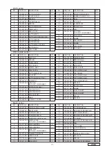
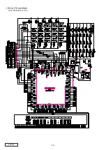
VRX630
R773
119-1011-15 1/16W 100 ohm
R774
119-1011-15 1/16W 100 ohm
R775
116-1021-15 1/8W 1k ohm
R776
119-3931-15 1/16W 39k ohm
R777
119-2731-15 1/16W 27k ohm
R778
116-1021-15 1/8W 1k ohm
R779
119-3931-15 1/16W 39k ohm
R780
119-2731-15 1/16W 27k ohm
R781
119-6821-15 1/16W 6.8k ohm
R782
119-4731-15 1/16W 47k ohm
R783
119-1831-15 1/16W 18k ohm
R784
119-1051-15 1/16W 1M ohm
R785
032-0140-89 1/10W 47k ohm F
R786
119-0000-05 1/16W 0 ohm JW
R787
032-0140-99 1/10W 39k ohm F
R788
119-5621-15 1/16W 5.6k ohm
R789
119-1521-15 1/16W 1.5k ohm
R790
032-0140-89 1/10W 47k ohm F
R791
119-3021-15 1/16W 3k ohm
R792
032-0140-99 1/10W 39k ohm F
R793
119-1011-15 1/16W 100 ohm
R794
119-1021-15 1/16W 1k ohm
R795
119-2221-15 1/16W 2.2k ohm
R796
119-3311-15 1/16W 330 ohm
R797
119-1011-15 1/16W 100 ohm
R798
119-6811-15 1/16W 680 ohm
R799
119-1011-15 1/16W 100 ohm
R800
119-5621-15 1/16W 5.6k ohm
R801
119-8221-15 1/16W 8.2k ohm
R802
119-1521-15 1/16W 1.5k ohm
R803
119-4741-15 1/16W 470k ohm
R804
119-4741-15 1/16W 470k ohm
R805
119-4741-15 1/16W 470k ohm
R806
119-4741-15 1/16W 470k ohm
R807
119-4741-15 1/16W 470k ohm
R808
119-6831-15 1/16W 68k ohm
R809
119-2221-15 1/16W 2.2k ohm
R810
119-1031-15 1/16W 10k ohm
R811
119-2211-15 1/16W 220 ohm
R812
119-1021-15 1/16W 1k ohm
R813
032-0092-43 1/10W 3.0k ohm F
R814
032-0092-43 1/10W 3.0k ohm F
R815
119-1011-15 1/16W 100 ohm
R816
119-1011-15 1/16W 100 ohm
R817
119-0000-05 1/16W 0 ohm JW
R818
119-1011-15 1/16W 100 ohm
R901
119-2711-15 1/16W 270 ohm
R902
119-2711-15 1/16W 270 ohm
R903
119-2711-15 1/16W 270 ohm
R904
119-2711-15 1/16W 270 ohm
S1
002-0313-91 THERMISTOR
S701
013-6100-00 SKHLLB
S702
013-7205-50 SPVE1-3
S902
013-6511-50 LS9J2M-1SR
S903
013-6511-50 LS9J2M-1SR
S904
013-6511-50 LS9J2M-1SR
S905
013-6511-50 LS9J2M-1SR
S906
013-9907-00 RKJXM1012
T701
007-1153-90 873AC-1071
T702
007-1152-00 BLC216HP
TH601
002-0216-95 DTN-T203K103KS
VR701
012-6009-52 1k ohm
VR702
012-6009-56 10k ohm
VR703
012-6009-58 33k ohm
VR704
012-6009-58 33k ohm
VR705
012-6009-58 33k ohm
VR706
012-6009-58 33k ohm
VR707
012-6009-58 33k ohm
VR708
012-6009-52 1k ohm
X701
061-1078-00 3.5795MHz
X702
061-3036-00 4.433619MHz
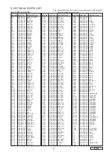
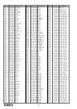
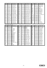
REF No. PART No.
DESCRIPTION
REF No. PART No.
DESCRIPTION
REF No. PART No.
DESCRIPTION
REF No. PART No.
DESCRIPTION
REF No. PART No.
DESCRIPTION
REF No. PART No.
DESCRIPTION
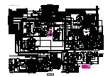
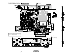
DCP PWB section(B4)
C901
178-1055-79 1uF
C902
178-1055-79 1uF
D901
001-7064-90 CL-170SR
D902
001-7064-90 CL-170SR
D903
001-7064-90 CL-170SR
D904
001-0525-90 IMN10
D905
001-0525-90 IMN10
D907
001-7046-00 NSPW310BS
D909
001-2601-90 MA728-TX
D910
001-2601-90 MA728-TX
D911
001-2601-90 MA728-TX
D912
001-0529-36 MA8062-H
D913
001-0529-36 MA8062-H
D914
001-0529-36 MA8062-H
D915
001-0529-36 MA8062-H
D916
001-0529-36 MA8062-H
D917
001-0529-36 MA8062-H
D918
001-0529-36 MA8062-H
D919
001-0529-36 MA8062-H
IC901
051-6001-01 uPD16431AGC-7ET
J901
076-0531-00 15P
L901
010-2323-71 33uH
Q901
125-0002-92 RN2402
Q902
125-2017-97 RN1427
Q903
125-0002-92 RN2402
Q904
125-2017-97 RN1427
R901
116-6811-15 1/8W 680 ohm
R903
116-6811-15 1/8W 680 ohm
R905
116-6811-15 1/8W 680 ohm
R907
116-6811-15 1/8W 680 ohm
R909
116-6811-15 1/8W 680 ohm
R911
116-6811-15 1/8W 680 ohm
R913
116-6811-15 1/8W 680 ohm
R914
119-1021-15 1/16W 1k ohm
R915
119-1021-15 1/16W 1k ohm
R916
119-4711-15 1/16W 470 ohm
R917
119-1021-15 1/16W 1k ohm
R918
119-1041-15 1/16W 100k ohm
R919
119-1021-15 1/16W 1k ohm
R920
119-1021-15 1/16W 1k ohm
R921
119-1021-15 1/16W 1k ohm
R922
119-1021-15 1/16W 1k ohm
R923
119-1031-15 1/16W 10k ohm
R924
119-1041-15 1/16W 100k ohm
R925
119-1511-15 1/16W 150 ohm
R926
119-1511-15 1/16W 150 ohm
R928
119-2221-15 1/16W 2.2k ohm
R929
119-2221-15 1/16W 2.2k ohm
S901
013-6511-50 LS9J2M-1SR
S902
013-6511-50 LS9J2M-1SR
S903
013-6511-50 LS9J2M-1SR
S904
013-6511-50 LS9J2M-1SR
S905
013-6511-50 LS9J2M-1SR
S906
013-6511-50 LS9J2M-1SR
S907
013-6312-50 SKRP-ABE-010
S908
013-6511-50 LS9J2M-1SR
S910
013-6511-50 LS9J2M-1SR
S911
013-6511-50 LS9J2M-1SR
S912
013-6511-50 LS9J2M-1SR
S913
013-6511-50 LS9J2M-1SR
S914
013-6511-50 LS9J2M-1SR
S915
013-6511-50 LS9J2M-1SR
S916
013-6511-50 LS9J2M-1SR
S917
013-6312-50 SKRP-ABE-010
S918
013-6511-50 LS9J2M-1SR
S919
013-6511-50 LS9J2M-1SR
S920
013-6511-50 LS9J2M-1SR
S921
013-6511-50 LS9J2M-1SR
S922
013-6511-50 LS9J2M-1SR


