CDB4923 CDB49300
DS262DB2
9
input ports of the DSP. These configuration allows
the user to drive signals on stake headers J11 and
J12 in order to operate the DSP as if it were part of
an embedded system. The user is responsible for
providing the appropriate clocking signals, control
signals, and data signals to the DSP in full external
mode, but the user only provides control signals in
exernal control mode.
In the external modes the audio output of the DSP
still drives the on-board DACs and digital transmit-
ters thus allowing the user to access the audio on
the analog and digital output connectors provided
by the CDB4923/300. The stake headers J11 and
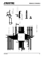
J12 can be found in Figure 4.
All on-board clocks and data lines are routed
through the PLD (U11) in order to provide maxi-
mum flexibility in the evaluation of different sys-
tem configurations. The PLD will perform all +5 V
to +3.3 V/+2.5 V conversions between the DSP
and the +5 V parts with which it interacts by con-
figuring the I/O power jumper (J63). The system
can also be configured in an external interface de-
scribed above. The external modes are detailed in
Data Selection. All PLD modes are selected using
DIP switch S3. The PLD (U11) and switch S3 are
shown in Figure 7.
A specialized IC (U12), the MAX708, has been in-
cluded on the CDB4923/300 in order to generate a
system reset at power-up, when the digital power
begins to fail, and when the system reset button
(SW1) is depressed. This chip helps to insure con-
sistent operation on the board by providing a
200 ms reset pulse whenever activated.
5. DATA SELECTION
Data selection on the CDB4923/300 refers to the
routing of audio data, audio clocks, control data,
and control clocks. Because the PLD plays such a
crucial role in determining the routing and control
scheme, each data selection mode is also referred to
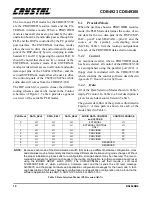
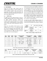
as a ‘PLD mode.’ It is important to note that Table
2, the PLD Mode table, is based directly upon the
version of the control PLD (U11) used on each par-
ticular board. Each PLD has a specific revision
code printed on its label. If your PLD version dif-
fers from the one described in this document, con-
tact the factory to determine which feature set is
provided with your board.
Analog
Output
Stereo
Analog In
Digital Output
Digital Input
Control
Interface
Patch Area
RESET
C
S
8414
PL
L
+3.3V
+2.5V
CS492x
CS493xx
OSC
PLD
CS8404A
CS8404A
CS8404A
CS4340
CS4340
CS4340
CS5334
CRD4923-MEM
CDB49300-MEM
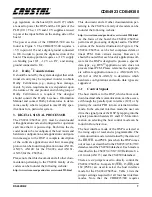
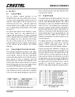
Figure 1. External Memory Example
Summary of Contents for CS492 Series
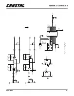
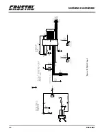
Page 18: ...CDB4923 CDB49300 18 DS262DB2 9 APPENDIX A SCHEMATICS Figure 4 CS492x CS493xx ...
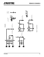
Page 19: ...CDB4923 CDB49300 DS262DB2 19 Figure 5 System Power ...
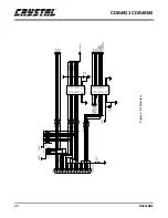
Page 20: ...CDB4923 CDB49300 20 DS262DB2 Figure 6 PC Interface ...
Page 21: ...CDB4923 CDB49300 DS262DB2 21 Figure 7 Control Logic ...
Page 22: ...CDB4923 CDB49300 22 DS262DB2 Figure 8 Clocking ...
Page 23: ...CDB4923 CDB49300 DS262DB2 23 Figure 9 Analog Input ...
Page 24: ...CDB4923 CDB49300 24 DS262DB2 Figure 10 Digital Input ...
Page 25: ...CDB4923 CDB49300 DS262DB2 25 Figure 11 D A Converters ...
Page 26: ...CDB4923 CDB49300 26 DS262DB2 Figure 12 Analog Output ...
Page 27: ...CDB4923 CDB49300 DS262DB2 27 Figure 13 Digital Output ...
Page 28: ...CDB4923 CDB49300 28 DS262DB2 Figure 14 Top Layer ...
Page 29: ...CDB4923 CDB49300 DS262DB2 29 Figure 15 Bottom Layer ...
Page 30: ...CDB4923 CDB49300 30 DS262DB2 Figure 16 SSTOP ...
Page 31: ...CDB4923 CDB49300 DS262DB2 31 Figure 17 ASYSTOP ...
Page 32: ...CDB4923 CDB49300 32 DS262DB2 Figure 18 Layer 2 ...
Page 33: ...CDB4923 CDB49300 DS262DB2 33 Figure 19 Layer 3 ...
Page 49: ... Notes ...
Page 50: ......


