CDB4923 CDB49300
6
DS262DB2
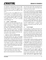
proper voltage), configure the audio decoder for
different host communication modes and select the
clock source for the DSP (internal PLL or external
clock). The stake headers provide a convenient lo-
cation for probing signal values and also serve as
the interface to the CRD4923-MEM (for use with
CS492x only) or CDB49300-MEM (for use with
the CS493xx only) external memory expander
cards.
The control interface of the CDB4923/300 is com-
posed of a 25 pin connector designed to accept a
parallel port cable, a programmable logic device
(PLD), and two TTL buffers designed to buffer the
sixteen signal lines coming from the PC. Using the
software provided with the demonstration board,
the user can download code to the DSP, configure
the application code running on the DSP, perform a
reset of the DSP, and deliver compressed audio
files to the DSP. An additional control interface is
provided on the J11 and J12 stake headers when the
PLD is placed into an external interface mode as
described in Data Selection.
The majority of the control logic for this board is
found in the PLD. The PLD latches all signals com-
ing from the parallel port interface, performs all I/O
routing on the board, and provides level conversion
from +5 V to +3.3 V/+2.5 V depending on the set-
ting of the I/O power jumper (J63) for the PLD. A
dip switch is used to control different data/clock
routing configurations. There is also an external re-
set chip (MAX708) which is responsible for system
reset at power-up and when the digital power be-
gins to fail.
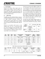
The sources for the main DSP clock on the
CDB4923/300 are the oscillator and the external
PLL. When the oscillator is chosen, the main DSP
clock frequency can be either the 27 MHz or
12.288 MHz oscillator provided with the board.
When properly configured the external PLL can
provide a processor clock frequency ranging from
33 MHz to 81 MHz. When the external PLL is used
for the DSP processor clock, it can also be used to
master the system oversampling clock, MCLK.
The CDB4923/300 features six channels of analog
output provided by three CS4340 DACs. The out-
puts are provide a 3.5 V
pp
signal, and each output
has protection circuitry to protect against speaker
’popping’. A DIP switch is provided for changing
the data format accepted by the CS4340.
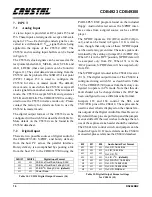
There is a stereo analog input on the CDB4923/300
which is designed to interface to line levels of up to
2 V
rms
. The analog to digital conversion is per-
formed by the CS5334. A DIP switch is provided
for changing the format of the audio data provided
by the CS5334.
Input and output ports are provided for S/PDIF dig-
ital audio streams (IEC60958 and IEC61937). An
incoming S/PDIF stream can be supplied either
with an optical cable or coaxial cable. The S/PDIF
outputs of the CDB4923/300 are all optical. The in-
formation from the AUDATA0-2 pins of the
CS492x are transmitted on AOUT_DIG0-2 using
digital audio interface transmitters (CS8404A).
Optical output J43 is connected directly to the
S/PDIF transmitter of the DSP. DIP switches are
provided for changing the serial audio format of the
data provided by the CS8414 and the data accepted
by the CS8404A.
The CDB4923/300 provides both analog and digi-
tal patch areas. The digital patch area provides ac-
cess to both +5 V and DSP Power (voltage of the
CS492x/CS493xx core). These patch areas are very
useful when prototyping circuit modifications.
They can also be used as a place to connect signal
buffers when using the CDB4923/300 in an exter-
nal interface mode.
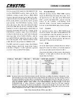
2.1
Power Requirements
This board is composed of about 75% digital logic
which is fed by the +5 V power supply. Since the
CS492x is a +3.3 V part and the CS493xx is a
+2.5 V part, there are also +3.3 V and +2.5 V volt-
Summary of Contents for CS492 Series
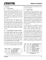
Page 18: ...CDB4923 CDB49300 18 DS262DB2 9 APPENDIX A SCHEMATICS Figure 4 CS492x CS493xx ...
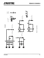
Page 19: ...CDB4923 CDB49300 DS262DB2 19 Figure 5 System Power ...
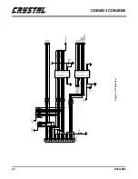
Page 20: ...CDB4923 CDB49300 20 DS262DB2 Figure 6 PC Interface ...
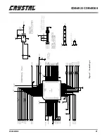
Page 21: ...CDB4923 CDB49300 DS262DB2 21 Figure 7 Control Logic ...
Page 22: ...CDB4923 CDB49300 22 DS262DB2 Figure 8 Clocking ...
Page 23: ...CDB4923 CDB49300 DS262DB2 23 Figure 9 Analog Input ...
Page 24: ...CDB4923 CDB49300 24 DS262DB2 Figure 10 Digital Input ...
Page 25: ...CDB4923 CDB49300 DS262DB2 25 Figure 11 D A Converters ...
Page 26: ...CDB4923 CDB49300 26 DS262DB2 Figure 12 Analog Output ...
Page 27: ...CDB4923 CDB49300 DS262DB2 27 Figure 13 Digital Output ...
Page 28: ...CDB4923 CDB49300 28 DS262DB2 Figure 14 Top Layer ...
Page 29: ...CDB4923 CDB49300 DS262DB2 29 Figure 15 Bottom Layer ...
Page 30: ...CDB4923 CDB49300 30 DS262DB2 Figure 16 SSTOP ...
Page 31: ...CDB4923 CDB49300 DS262DB2 31 Figure 17 ASYSTOP ...
Page 32: ...CDB4923 CDB49300 32 DS262DB2 Figure 18 Layer 2 ...
Page 33: ...CDB4923 CDB49300 DS262DB2 33 Figure 19 Layer 3 ...
Page 49: ... Notes ...
Page 50: ......


