background image

3-17

Copyright 2009 Cirrus Logic, Inc.

DS734UM7

SPI Port

CS485xx Hardware User’s Manual

 3.3.1.2 SPI Messaging

Messaging to the CS485xx using the SPI bus requires usage of all the information provided in the SPI Bus 

Description and Bus Dynamics above. For control and application image downloading, SPI transactions to 
the CS485xx will involve 4-byte words. A detailed description of the serial SPI communication mode is 
provided in this section. This includes:

A flow diagram and description for a serial SPI write

A flow diagram and description for a serial SPI read 

 3.3.1.3 Performing a Serial SPI Write

Information provided in this section is intended as a functional description indicating how to perform an SPI 
write from an external device (master) to the CS485xx DSP (slave). The system designer must ensure that 
all timing constraints of the SPI Write Cycle are met (see the CS485xx datasheet for timing specifications). 
When performing an SPI write, the same protocol is used whether writing single-word messages to the boot 
firmware, writing multiple-word overlay images to the boot firmware, or writing multiple-word messages to 
the application firmware. The example shown in this section can be generalized to fit any SPI write situation. 

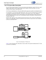
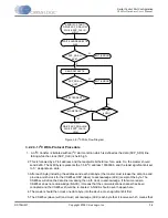
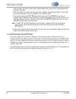
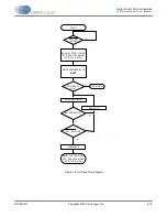
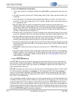
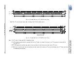
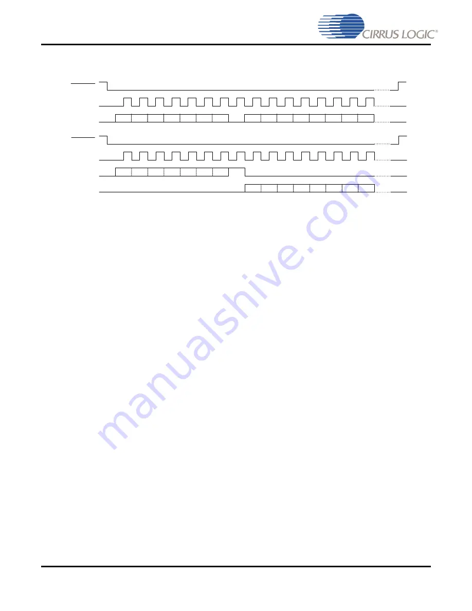
The flow diagram shown in 

Figure 3-15 

, illustrates the sequence of events that define the SPI write protocol. 

This protocol is discussed in the high-level procedure in 

Section 3.3.1.3.1

SCP_CLK

SCP_MOSI

7-bit SPI Address

Data Byte

SCP_CS

R/W

SCP_CLK

SCP_MOSI

Data Byte

SCP_CS

SCP_MISO

R/W

7-bit SPI Address

Summary of Contents for CS485 Series

Page 1: ...Copyright 2009 Cirrus Logic AUG 09 DS734UM7 CS485xx 32 bit Audio DSP Family http www cirrus com CS485xx Hardware User s Manual ...

Page 2: ... All other brand and product names in this document may be trademarks or service marks of their respective owners Dolby Dolby Digital Dolby Headphone Dolby Virtual Speaker AC 3 Pro Logic and Audistry are registered trademarks of Dolby Laboratories Inc AAC Dolby Headphone2 Dolby Virtual Speaker2 and Dolby Digital Surround EX are trademarks of Dolby Laboratories Inc Supply of an implementation of Do...

Page 3: ... 3 12 Clock Manager and PLL 1 9 1 3 13 Programmable Interrupt Controller 1 10 Chapter 2 Operational Modes 2 1 2 1 Introduction 2 1 2 2 Operational Mode Selection 2 2 2 3 Slave Boot Procedures 2 2 2 3 1 Slave Boot 2 3 2 3 2 Performing a Slave Boot 2 3 2 3 2 1 Slave Boot Procedure 2 5 2 3 3 Boot Messages 2 6 2 3 3 1 Slave Boot 2 6 2 3 3 2 Soft Reset 2 6 2 3 3 3 Messages Read from CS485xx 2 6 2 4 Mas...

Page 4: ...mat 4 5 4 2 3 2 Left Justified Format 4 6 4 3 DAI Hardware Configuration 4 6 4 3 1 DAI Hardware Naming Convention 4 6 Chapter 5 Direct Stream Data DSD Input Interface 5 1 5 1 Digital Audio Input Port Description 5 1 5 1 1 DSD Pin Description 5 1 5 1 2 Supported DSD Functional Blocks 5 1 Chapter 6 Digital Audio Output Interface 6 1 6 1 Introduction 6 1 6 2 Digital Audio Output Port Description 6 1 ...

Page 5: ... 10 Figure 2 6 Flowchart of Steps Used to Exit Low Power Mode 2 13 Figure 3 1 Serial Control Port Internal Block Diagram 3 2 Figure 3 2 Block Diagram of I2 C System Bus 3 3 Figure 3 3 I2 C Start and Stop Conditions 3 4 Figure 3 4 I2 C Address with ACK and NACK 3 5 Figure 3 5 Data Byte with ACK and NACK 3 6 Figure 3 6 Stop Condition with ACK and NACK 3 6 Figure 3 7 Repeated Start Condition with ACK...

Page 6: ... channels of Digital Audio Input All Audio Clocks Synchronous to S PDIF RX 8 2 Figure 8 2 I2 C Slave 10 Channels of Digital Audio Input Dual Clock Domains Output Audio Clocks Synchronous to HDMI Rx 8 3 Figure 8 3 I2 C Slave 12 Channels of Digital Audio Input Single Clock Domain All Audio Clocks Synchronous to XTAL_OUT 8 4 Figure 8 4 I2 C master 10 Channels of Digital Audio Input All Audio Clocks S...

Page 7: ...4 Input LRCLK Polarity Configuration Input Parameter C 4 8 Table 4 5 DAI2_DATA Clock Source Input Parameter E 4 9 Table 4 6 DAI1_DATA Clock Source Input Parameter F 4 9 Table 4 7 Chip Version Input Parameter G 4 9 Table 4 8 DAII TDM Input Parameter H 4 9 Table 5 1 DSDl Audio Input Port 5 1 Table 6 1 Digital Audio Output DAO Pins 6 1 Table 6 2 Output Clock Mode Configuration Parameter A 6 5 Table 6...

Page 8: ... PLL Filter Pins 8 12 Table 8 6 Reference PLL Component Values 8 12 Table 8 7 DSP Core Clock Pins 8 13 Table 8 8 Reset Pin 8 14 Table 8 9 Hardware Strap Pins 8 14 Table 8 10 Pin Assignments of CS48560 8 18 Table 8 11 Pin Assignments of CS48540 8 19 Table 8 12 Pin Assignments of CS48520 8 20 ...

Page 9: ...l necessary peripherals required to support the latest standards in consumer entertainment products In addition external serial Flash memory can be attached to the serial control port SCP for storage of run time parameters or as a boot ROM for custom applications This device is suitable for a variety of high performance audio applications These include Digital TVs Car Audio Head Units and Amplifie...

Page 10: ...put Stereo Audio Output Stereo Audio Output or SPDIF Transmitter DAO Controller ROM SRAM Timers GPIOs Clock Manager and PLL Serial Control Port Debug Controller DAO1 Stereo Audio Input DSD Stereo Audio Input DSD Stereo Audio Input DSD Stereo Audio Input DSD DAI1 CS48560 Stereo Audio Input DSD Stereo Audio Input DSD DAI2 DAI Controller X Stereo Audio Output Stereo Audio Output DMA Controller with 8...

Page 11: ...Y P X P Y 64 bit Stereo Audio Output Stereo Audio Output Stereo Audio Output SPDIF Transmitter DAO Controller ROM SRAM Timers GPIOs Clock Manager and PLL Serial Control Port Debug Controller DAO1 Stereo Audio Input Stereo Audio Input Stereo Audio Input DAI1 CS48540 Stereo Audio Input DAI2 DAI Controller X Stereo Audio Output DMA Controller with 8 Channels Programmable Interrupt Controller Memory C...

Page 12: ...Programming Kit Please refer to the Related Documents section of this manual for additional application note information The CS485xx supports master mode interface on the serial control port to interface to SPI and I2 C serial FLASH chips thus allowing products to be field upgraded as new audio algorithms are developed DAI Controller Peripheral Bus Controller Log Exp Security Ext 64 bit DMABus Per...

Page 13: ...se modules increase the number of valid channels in the audio I O buffer Virtualizer processor Any module that encodes PCM data into fewer output channels than input channels nÖ2 channels with the effect of providing phantom speakers to represent the physical audio channels that were eliminated Examples are Dolby Headphone and Dolby Virtual Speaker Generally speaking these modules reduce the numbe...

Page 14: ...ng a PC host to the debug port on the DSP The debug port consists of two modules an I2 C slave and a debug master The DBC master sends dedicated signals into the DSP core to initiate debug actions and it receives acknowledge signals from the core to indicate the requested action has been taken Basically this interface allows the DBC to insert instructions into the pipeline The core will acknowledg...

Page 15: ...eneral Purpose I O A 17 bit general purpose I O GPIO port is provided on the CS485xx chip to enhance system flexibility Many of the functional pins can be used for either GPIO or other peripheral functions Each GPIO pin can be individually configured as an output an input or an input with interrupt A GPIO interrupt can be triggered on a rising edge 0 to 1 transition falling edge 1 to 0 transition ...

Page 16: ...t by the DSP before the counter expires or the entire chip is reset This peripheral ensures that the CS485xx will reset itself in the event of a temporary system failure In standalone mode that is no host microcontroller MCU is present the DSP will reboot from external FLASH In slave mode that is host MCU present a GPIO will be used to signal the host that the watchdog has expired and the DSP shou...

Page 17: ...priority Each interrupt has a corresponding interrupt address that is also supplied to the DSP core The interrupt address is the same as the IRQ number interrupt 0 uses interrupt address 0 and interrupt 15 uses interrupt address 15 Both an enable mask and a run mask are provided for each interrupt The enable mask allows the enabled interrupts to generate a PIC_REQ signal to the DSP core and the ru...

Page 18: ...Functional Overview of the CS485xx Chip CS485xx Hardware User s Manual DS734UM7 Copyright 2009 Cirrus Logic Inc 1 10 ...

Page 19: ...oot device In Slave Boot Mode the CS485xx is the slave boot device and requires the system host controller the master boot device to load the application code Please see Figure 2 1 Thus there are two boot modes for the CS485xx Master Boot From serial SPI or I2 C FLASH EEPROM Slave Boot Using SPI or I2 C When the CS485xx is configured for an operational mode where it is the slave boot device one of...

Page 20: ...a a In I2C master mode the Image Start address 0x0 is sent as a 16 bit value with the default I2C address of 0x50 I2C clock frequency Fdclk 72 CS485xx I2C External ROM X 1 0 0 0 Master SPI 1 b b SPI master mode 1 is to support the legacy 16 bit SPI EEPROM The following defaults are used SPI Command Byte 0x03 Image Start address 0x0 is sent as a 16 bit value no dummy bytes SPI clock frequency Fdclk...

Page 21: ...nitially booting the DSP Typically this time is less than 200 ms If a message is sent to the DSP during this time the SCP_BSY pin will go low to indicate that the DSP is busy Any messages sent when the SCP_BSY pin is LOW will be lost If the SCP_BSY pin stays LOW longer than 200 ms the host must reboot the DSP 2 3 1 Slave Boot The Slave Boot procedure is a sequence in which the external host is the...

Page 22: ... SLAVE_BOOT READ_ MSG EXIT ERROR N Y MSG BOOT_SUCCESS EXIT ERROR N Y READ_ MSG MSG APP_START WRITE_ SOFT_RESET READ_ MSG EXIT ERROR N Y MORE ULD FILES Y N DONE SEND HARDWARE CONFIGURATIONS SEND FIRMWARE CONFIGURATIONS WRITE_ KICKSTART START RESET LOW SET HS 3 0 PINS FOR OPERATIONAL MODE is replaced with SPI I2C etc depending on the communication protocol used SEND ULD FILE ...

Page 23: ...read by the DSP is corrupted The communications interface hardware and code image integrity should be checked if this occurs 8 Repeat steps 2 7 for all code images overlays The host repeats these steps until all overlays for the application have been successfully loaded See the application note for more information on the overlays necessary at start up 9 Send the SOFT_RESET message After reading t...

Page 24: ...sage is the message sent to the CS485xx after all of the overlays have been successfully booted The SOFT_RESET leaves execution of the bootloader and begins execution of the loaded overlays The overlays can be configured once the SOFT_RESET message has been sent 2 3 3 3 Messages Read from CS485xx Table 2 4 defines the boot read messages in mnemonic and actual hex value used in CS485xx boot sequenc...

Page 25: ...e CS485xx will load a single overlay from address 0x0 It should be noted that the loaded overlay must reconfigure one of the control ports to be slave to the bus for a system host controller to configure the part Thus this type of boot process will be useful in systems without a system host controller or with a simple controller that only performs a monitoring task Currently this mode is not used ...

Page 26: ...ires that the host send or re send the hardware and software configuration messages 2 5 1 Softboot Messaging Two messages are relevant to the softboot procedure for the CS485xx These messages are SOFTBOOT and SOFTBOOT_ACK The SOFTBOOT message is sent from the host controller to the CS485xx to indicate to the CS485xx that the system requires swapping of overlays The SOFTBOOT_ACK is sent from the CS...

Page 27: ...ed to step 4 If the message is not the SOFTBOOT_ACK message the host should return to step 2 4 Load Overlays Repeat the boot procedure used to originally load the overlays into the CS485xx i e SLAVE_BOOT but only the overlays that need to be swapped should be loaded Skip the hard reset sequence starting the boot procedure from Step 2 Please note that this includes re downloading all hardware and s...

Page 28: ... the TIMEOUT period has been reached the host should exit If the IRQ pin is LOW proceed to step 3 MSG BOOT_START WRITE_ SLAVE_BOOT READ_ MSG N Y MSG BOOT_SUCCESS N Y READ_ MSG MSG APP_START WRITE_ SOFT_RESET READ_ MSG N Y MORE ULD FILES Y N DONE SEND HARDWARE CONFIGURATIONS SEND FIRMWARE CONFIGURATIONS WRITE_ KICKSTART is replaced with SPI I2C etc depending on the communication protocol used EXIT ...

Page 29: ...ode image integrity should be checked if this occurs 10 Repeat steps 4 8 for all code images Overlays The host repeats these steps until all overlays for the application have been successfully loaded See the application note for more information on the overlays necessary at start up 11 Send the SOFT_RESET message After reading the BOOT_SUCCESS message on the last code image overlay the host must s...

Page 30: ...e is no response Additionally all the GPIO pins will be set to inputs in low power mode with weak pull ups so there state can be checked to verify low power mode is active 2 6 3 Getting Out of Low Power Mode Follow these steps to get out of low power mode 1 Set DSP_RESET low 2 Set DSP_RESET high 3 Send the SLAVE_BOOT message 0x80000000 4 Read the BOOT_START message 0x00000001 5 Send the WAKEUP_ UL...

Page 31: ...t Low Power Mode Y Y N Y Y SET DSP_RESET LOW SET DSP_RESET HIGH WRITE_ SLAVE_BOOT MSG BOOT_START READ_ MSG EXIT ERROR SEND ULD FILE MSG BOOT_SUCCESS READ_ MSG EXIT ERROR WRITE_ SOFT_RESET N MSG APP_START READ_ MSG EXIT ERROR SEND HARDWARE CONFIGURATIONS N WRITE_ KICKSTART DONE Send uld from Table 2 8 SEND SOFTWARE CONFIGURATIONS Start ...

Page 32: ...xb485aa01 0x01000359 0x00000001 0x00000000 0xffffffff 0x427a0e9b WAKEUP_P4 ULD0x 0x08004409 0x00000002 0x00000001 0xb485aa01 0x01000359 0x00000001 0x00000000 0xffffffff 0x427a0e9a WAKEUP_P6 ULD 0x08004409 0x00000002 0x00000002 0xb485aa01 0x01000359 0x00000001 0x00000000 0xffffffff 0x427a0e99 WAKEUP_P8 ULD 0x08004409 0x00000002 0x00000003 0xb485aa01 0x01000359 0x00000001 0x00000000 0xffffffff 0x427...

Page 33: ...ce between the two is the actual protocol being implemented between the CS485xx and the host In addition the I2C slave has a true I2C mode that utilizes data flow mechanisms inherent to the I2C protocol If this mode is enabled the I2C slave will hold SCP_CLK low to delay a transfer as needed this is in addition to activating SCP_BSY 3 2 Serial Control Port Configuration The serial control port con...

Page 34: ...essable external devices Each external device interfaced to the CS485xx I2C port has the ability to communicate directly with the other devices and is assigned a unique address whether it is a CPU memory or some other device A block diagram of the CS485xx I2C Serial Control Port is provided in Figure 3 1 Figure 3 1 Serial Control Port Internal Block Diagram I2C Control Clocking SCP_BSY SCP_IRQ LSB...

Page 35: ...signals on the I2 C bus is always the responsibility of master devices each master generates its own clock signals when transferring data on the bus Bus clock signals from a master can only be altered when they are stretched by a slow slave device holding down SCP_CLK Both SCP_SDA and SCP_CLK are bidirectional lines When the bus is free both lines are pulled high by resistors The output stages of ...

Page 36: ...nd Stop Conditions Table 3 1 Serial Control Port 1 I2C Signals Pin Name Pin Description LQFP 48 Pin Pin Type SCP_CLK I2C Control Port Bit Clock In master mode this pin serves as the serial control clock output open drain in I2C mode output in SPI mode In serial slave mode this pin serves as the serial control clock input In I2C slave mode the clock can be pulled low by the port to stall the master...

Page 37: ...C Address with ACK and NACK For write operations the R W bit must be set to zero R W 0 Address 0x80 After the 8 bit data byte has been clocked the master will release the SCP_SDA line If the slave received the byte correctly it will drive the SCP_SDA line low for the next bit clock to acknowledge ACK that the data was received If the data was not received correctly the slave can communicate this b...

Page 38: ...te byte of data until it has performed some other function for example servicing an internal interrupt it can hold the SCP_CLK line low to force the master into a wait state Data transfer then continues when the slave is ready for another byte of data and releases SCP_CLK Start SCP_CLK SCP_SDA A 6 A 5 A 4 A 3 A 2 A 1 A 0 R W ACK Data Byte ACK M S M S Write M S S M Read Start SCP_CLK SCP_SDA A 6 A ...

Page 39: ...spended transaction may continue It is important for the host to obey the SCP_BSY pin status for proper communication with the DSP 3 2 2 3 Performing a Serial I2 C Write Information provided in this section is intended as a functional description indicating how to use the configured serial control port to perform a I2C write from an external device master to the CS485xx DSP slave The system design...

Page 40: ...e the master must release the data line and provide a ninth clock for the CS485xx DSP slave to acknowledge ACK receipt of the byte The CS485xx will drive the data line low during the ninth clock to acknowledge If for some reason CS485xx does not acknowledge NACK it means that the communications channel has been corrupted and the CS485xx should be re booted A NACK should never happen here 4 The mas...

Page 41: ...lock stretching to indicate that the host should pause communication So the host has the option of checking for SCP_CLK held low rather than SCP_BSY low 8 At the end of a data transfer a stop condition must be sent The stop condition is defined as the rising edge of SCP_SDA while SCP_CLK is high 3 2 2 4 Performing a Serial I2 C Read Information provided in this section is intended as a functional ...

Page 42: ...Logic Inc 3 10 Figure 3 9 I2C Read Flow Diagram SCP_IRQ LOW BYTES READ 4 Y N N Y SEND I2C STOP DRIVE SCP_SDA HIGH WHILE SCP_CLK IS HIGH SCP_IRQ LOW Y N START SEND I2C START DRIVE SCP_SDA LOW WHILE SCP_CLK IS HIGH WRITE ADDRESS BYTE 0x81 READ DATA BYTE SEND ACK SEND NACK SCP_SDA ACK Y N EXIT ERROR ...

Page 43: ...w after reading a 4 byte word proceed to step 7 If SCP_IRQ has risen proceed to step 9 9 The master should let the SCP_SDA line stay high for the 9th SCP_CLK clock as a no acknowledge NACK to CS485xx This followed by an I2C stop condition SCP_SDA driven high while SCP_CLK is high signals an end of read to CS485xx See the next section SCP_IRQ Behavior for the an in depth explanation of SCP_IRQ 3 2 ...

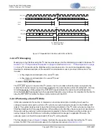
Page 44: ...saction is responsible for providing ACK 3 SCP_IRQ remains low until the rising edge of the clock for the last bit of the last byte read from the I2 C slave 4 A NACK is sent by the master after the last byte to indicate the end of the read cycle This must be followed with an I2C Stop condition or I2C Repeated Start condition Start SCP_CLK SCP_SDA Data Byte 3 MSB Stop 7 bit Address R W A C K A C K ...

Page 45: ...ata SCP_MISO Although the separate data I O lines provide full duplex capabilities the CS485xx chip only uses a half duplex SPI bus Each device on the bus may respond to one or more unique commands and can operate as either a transmitter or receiver A device is considered the master in a transaction if it drives the CS pin of another device and is also mastering the SCP_CLK line A block diagram of...

Page 46: ...nput signal In SPI serial master mode if this pin is driven low by another master device on the bus it will cause a mode fault to occur 38 Input SCP_CLK SPI Control Port Bit Clock In master mode this pin serves as the serial control clock output In serial slave mode this pin serves as the serial control clock input 36 I O SCP_MOSI SPI Mode Master Data Output Slave Data Input SCP_MOSI in SPI slave ...

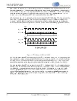
Page 47: ...lity to accept or supply bytes on the bus at the rate at which the master is driving SCP_CLK All data put on the SCP_MOSI and SCP_MISO lines must be in 8 bit bytes The number of bytes that can be transmitted per transfer is unrestricted Data is transferred with the most significant bit MSB first For the CS485xx slave SPI port the first byte is an address byte that must always be sent by the master...

Page 48: ...ndicates the master must halt transmission Once the SCP_BSY signal goes high the suspended transaction may continue The host must obey the SCP_BSY pin or control data will be lost SCP_CLK SCP_MOSI 7 bit SPI Address Data Byte SCP_CS R W SCP_CLK SCP_MOSI Data Byte SCP_CS SCP_MISO R W 7 bit SPI Address SCP_CLK SCP_MOSI 7 bit SPI Address Data Byte SCP_CS R W SCP_CLK SCP_MOSI Data Byte SCP_CS SCP_MISO ...

Page 49: ...cription indicating how to perform an SPI write from an external device master to the CS485xx DSP slave The system designer must ensure that all timing constraints of the SPI Write Cycle are met see the CS485xx datasheet for timing specifications When performing an SPI write the same protocol is used whether writing single word messages to the boot firmware writing multiple word overlay images to ...

Page 50: ...or each byte 4 If the master has no more data words to write to the CS485xx then proceed to step 6 If the master has more data words to write to the CS485xx then proceed to step 5 5 The master should poll the SCP_BSY signal until it goes high If the SCP_BSY signal is low it indicates that the CS485xx is busy performing some task that requires halting the serial control port Once the CS485xx is abl...

Page 51: ...nsaction is initiated by the CS485xx slave driving SCP_IRQ low to indicate that it has data to be read 2 The master begins a SPI transaction driving chip select SCP_CS low 3 This is followed by a 7 bit address and the read write bit set high for a read So the master should send 0x81 The 0x81 byte represents the 7 bit SPI address 1000000b and the least significant bit set to 1 designates a read 4 A...

Page 52: ...7 Copyright 2009 Cirrus Logic Inc 3 20 5 If SCP_IRQ is still low after 4 bytes then proceed to step 4 and read another 4 bytes out of the CS485xx slave 6 If SCP_IRQ is high the SCP_CS line of CS485xx should be driven high to end the read transaction ...

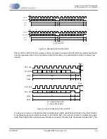
Page 53: ...the last byte to be read from the SPI slave 2 After going high IRQ remains high until the CS signal is raised to end the SPI transaction If there are more bytes to read IRQ will fall after CS has gone high SCP_CLK SCP_MOSI Data Byte 3 MSB 7 bit Address R W Data Byte 2 Data Byte 1 Data Byte 0 LSB SCP_CS S C P _ C L K S C P _ M O S I D a t a B y t e 3 M S B 7 b i t A d d r e s s R W D a t a B y t e ...

Page 54: ... out of CS485xx If there is no more data to be transferred SCP_IRQ will go high at this point After going high SCP_IRQ is guaranteed to stay high until the rising edge of SCP_CS This end of transfer condition signals the master to end the read transaction by clocking the last data bit out of CS485xx and then driving the CS485xx SCP_CS line high to signal that the read sequence is over If SCP_IRQ i...

Page 55: ... input pins up to 10 channels total or six digital audio pins up to 12 channels depending on the mode of operation configured The pins can be configured to load audio samples in a number of formats or accept multiple stereo channels on a single input pin DAI features include Five Digital Audio Input Pins Capable of Supporting Many Audio Formats with Dual Clock Domains on CS48560 Four Digital Audio...

Page 56: ...nput Data 0 PCM Audio Input Data 0 Serial data input that can accept PCM audio data that is synchronous to DAI_SCLK1 DAI_LRCLK1 or DAO_SCLK DAO_LRCLK 10 Input DAI1_DATA1 PCM Audio Input Data Note DAI1_DATA1 is not available on CS48520 11 Input DAI1_DATA2 PCM Audio Input Data Note DAI1_DATA2 is not available on CS48520 13 Input DAI1_DATA3 PCM Audio Input Data Note DAI1_DATA3is not available on CS48...

Page 57: ...supported with the CS48560 DAI Figure 4 1 10 Channel DAI Port Block Diagram Figure 4 2 shows the functional block diagram of the features currently supported with the CS48540 DAI Figure 4 2 8 Channel DAI Port Block Diagram Figure 4 3 shows the functional block diagram of the features currently supported with the CS48520 DAI DAI1_DATA0 DMA to Peripheral Bus DAI1_DATA0 DAI1_DATA1 DAI1_DATA1 DAI1_DAT...

Page 58: ... clock domain The firmware currently available can operate on only one of these input ports at a time providing for stereo PCM processing or multichannel PCM processing Please see AN298 for details on configuring the firmware to select these different inputs 4 2 2 2 Single Clock Domain 12 Channel Input The DAI can also be configured to accept up to 12 channels of linear PCM audio 6 serial audio da...

Page 59: ...xx supports It should be noted that the input ports use up to 32 bit PCM resolution 4 2 3 1 I2 S Format Figure 4 5 illustrates the I2 S format For I2 S data is presented most significant bit MSB first one SCLK delay after the transition of DAIn_LRCLK and is valid on the rising edge of DAIn_SCLK For the I2S format the left subframe is presented when DAIn_LRCLK is low and the right subframe is prese...

Page 60: ...e see AN298 CS485xx Firmware User s Manual for more information on kickstarting In general the hardware configuration can only be changed immediately after download or after soft reset Hardware configuration messages are used to physically reconfigure the hardware of the audio decoder as when enabling or disabling address checking for the serial communication port Hardware configuration messages a...

Page 61: ...n message only one hex message should be sent per parameter Table 4 2 Input Data Format Configuration Input Parameter A A Value Data Format Hex Message 0 default I2S 24 bit 0x81800010 0xFFFF0000 0x81400010 0x01001F00 0x81800011 0xFFFF0000 0x81400011 0x01001F00 0x81800012 0xFFFF0000 0x81400012 0x01001F00 0x81800013 0xFFFF0000 0x81400013 0x01001F00 0x81800014 0xFFFF0000 0x81400014 0x01001F00 1 Left ...

Page 62: ...xFFDFFFFF 0x81800014 0xFFDFFFFF 1 Data Clocked in on SCLK Falling Edge 0x81400010 0x00200000 0x81400011 0x00200000 0x81400012 0x00200000 0x81400013 0x00200000 0x81400014 0x00200000 Table 4 4 Input LRCLK Polarity Configuration Input Parameter C C Value LRCLK Polarity Both DAI and CDI Port HEX Message 0 default LRCLK Low indicates Channel 0 i e Left 0x81800010 0xFFDFFFFF 0x81800011 0xFFDFFFFF 0x8180...

Page 63: ...urce HEX Message 0 default DAI1_LRCLK DAI1_SCLK 0x81800015 0xF00FFFFF 1 DAI2_LRCLK DAI2_SCLK 0x81400015 0x05500000 0x81800015 0xF55FFFFF Table 4 7 Chip Version Input Parameter G G Value Chip Version HEX Message 0 CS48520 0x81400015 0x00080000 0x81800015 0xFFF80000 1 CS48540 0x81400015 0x00088800 0x81800015 0xFFF88800 2 CS48560 0x81400015 0x0008D100 0x81800015 0xFFF8D100 Table 4 8 DAII TDM Input Pa...

Page 64: ...are Configuration CS485xx Hardware User s Manual DS734UM7 Copyright 2009 Cirrus Logic Inc 4 10 a TDM Time Division Multiplex is only available on the CS48560 product b Accepts a maximum of 12 channlels of input ...

Page 65: ...igned to accept DSD audio data from up to 6 pins simultaneously 6 channels total DSD features include Up to Six DSD Input Pins One Shared DSD_CLK for All Data Pins Supports 44 1 kHz and 88 2 kHz Sample Rates 5 1 1 DSD Pin Description Table 5 1 shows the mnemonic and pin description of the pins associated with the DSD port on CS48560 5 1 2 Supported DSD Functional Blocks Figure 5 1 below shows the ...

Page 66: ...S485xx Hardware User s Manual DS734UM7 Copyright 2009 Cirrus Logic Inc 5 2 Figure 5 1 DSD Port Block Diagram on CS48560 DSD_DATA0 DMA to Peripheral Bus DSD0 DSD_DATA1 DSD1 DSD_DATA2 DSD2 DSD_DATA3 DSD3 DSD_DATA4 DSD_CLK DSD4 DSD_DATA5 DSD5 ...

Page 67: ...these clocks if MCLK is provided The port supports data rates from 32 kHz to 192 kHz One DAO pin can also be configured to provide a 32 kHz to 192 kHz S PDIF transmitter XMTA output Figure 6 1 Figure 6 2 Figure 6 3 illustrate the DAO block diagrams for the CS48560 CS48540 and CS48520 products respectively 6 2 Digital Audio Output Port Description 6 2 1 DAO Pin Description Table 6 1 identifies the ...

Page 68: ... or 512Fs clock where Fs is the output sample rate DAO_SCLK is the bit clock used to clock data out on DAOn_DATA n DAO_LRCLK is the data framing clock whose frequency is equal to the sampling frequency for the DAO data outputs DAOn_DATA n are the data outputs and are typically configured for outputting two channels of I2S or left justified PCM data Figure 6 1 CS48560 DAO Block Diagram DAO1_DATA0 P...

Page 69: ...nual Figure 6 2 CS48540 DAO Block Diagram Figure 6 3 CS48520 DAO Block Diagram DAO1_DATA0 Peripheral Bus to DMA DAO1_DATA1 DAO1_DATA2 XMTA DAO2_DATA0 Clock Manager DAO_MCLK DAO_SCLK DAO_LRCLK SPDIF ENCODER DAO1_DATA0 Peripheral Bus to DMA DAO2_DATA0 Clock Manager DAO_MCLK DAO_SCLK DAO_LRCLK XMTA SPDIF ENCODER ...

Page 70: ... this format data is presented most significant bit MSB first one DAO_SCLK delay after the transition of DAO_LRCLK and is valid on the rising edge of DAO_SCLK The left subframe is presented when DAO_LRCLK is low and the right subframe is presented when DAO_LRCLK is high Figure 6 4 provides details on I2S compatible maximum of 32 bits serial audio formats Figure 6 4 I2S Compatible Serial Audio Form...

Page 71: ...arity G DAO TDM Table 6 2 Table 6 3 Table 6 4 Table 6 5 Table 6 6 Table 6 7 and Table 6 8 show the different values for each parameter as well as the hex message that needs to be sent to configure the port When creating the hardware configuration message only one hex message should be sent per parameter Table 6 2 shows values and messages for DAO output clock mode configuration parameters Table 6 ...

Page 72: ...locks 0x8140001B 0x00002000 Table 6 4 Output DAO_SCLK LRCLK Configuration Parameter C C Value DAO_SCLK Frequency Hex Message 0 default DAO_MCLK 256 FS DAO_SCLK DAO_MCLK 4 64 FS DAO_LRCLK DAO_SCLK 64 FS 0x8100002D 0x00007711 0x8100002E 0x00007711 0x8180001C 0xFFFFFF8F 0x8140001C 0x00000020 1 DAO_MCLK 256 FS DAO_SCLK DAO_MCLK 2 128 FS DAO_LRCLK DAO_SCLK 128 FS 0x8100002D 0x00017701 0x8100002E 0x0001...

Page 73: ... DAO_SCLK 128 FS 0x8100002D 0x00017711 0x8100002E 0x00017711 0x8180001C 0xFFFFFF8F 0x8140001C 0x00000040 7 DAO_MCLK 512 FS DAO_SCLK DAO_MCLK 2 256 FS DAO_LRCLK DAO_SCLK 256 FS 0x8100002D 0x00037701 0x8100002E 0x00037701 0x8180001C 0xFFFFFF8F 0x8140001C 0x00000060 8 DAO_MCLK 384 FS DAO_SCLK DAO_MCLK 4 96 FS DAO_LRCLK DAO_SCLK 96 FS 0x8100002D 0x00037211 0x8100002E 0x00037211 0x8180001C 0xFFFFFF8F 0...

Page 74: ... 0x00000001 0x81000022 0x00000001 0x81000023 0x00000001 0x81000024 0x00000001 0x81000025 0x00000001 0x81000026 0x00000001 0x81000027 0x00000001 1 Left Justified 32 bit 0x81000020 0x00000000 0x81000021 0x00000000 0x81000022 0x00000000 0x81000023 0x00000000 0x81000024 0x00000000 0x81000025 0x00000000 0x81000026 0x00000000 0x81000027 0x00000000 0x8180001c 0xFFFFFBFF 0x8180001d 0xFFFFFBFF 2 TDM 32 bit...

Page 75: ...ut Default S PDIF Transmitter Sent configuration from Table 6 10 Table 6 6 Output DAO_LRCLK Polarity Configuration Parameter E E Value DAO_LRCLK Polarity Hex Message 0 default LRCLK Low indicates Left Subchannel 0x8140001C 0x00000700 0x8140001D 0x00000700 1 LRCLK Low indicates Right Subchannel 0x8180001C 0xFFFFFBFF 0x8140001C 0x00000300 0x8180001D 0xFFFFFBFF 0x8180001D 0x00000300 Table 6 7 Output ...

Page 76: ...red as S PDIF Transmitter Sent configuration from Table 6 10 A soft reset is required when switching between any of the above modes Table 6 9 S PDIF Transmitter Pins Pin Name Pin Description LQFP 48 Pin Pin Type DAO_DATA3 XMTA S PDIF Audio Output A 29 Output Table 6 10 S PDIF Transmitter Configuration Description Hex Message Enable S PDIF Audio Output A on DAO_DATA3 XMTA 0x8100001e 0x00005080 ...

Page 77: ...pecific to each crystal The CS485xx Data Sheet specifies acceptable crystal parameters including CL and ESR When a crystal is used XTAL_OUT may be used to clock other devices in the system such as an external S PDIF receiver Table 7 1 describes the XTAL_OUT XTI and XTO pins The PLL is controlled by the clock manager in the DSP O S application software AN298 CS485xx Firmware User s Manual should be...

Page 78: ...AN298 CS485xx Firmware User s Manual for more information on kickstarting In general the hardware configuration can only be changed immediately after download or after soft reset Hardware configuration messages are used to configure the XTAL_OUT divider 7 2 1 Crystal Oscillator Hardware Configuration Messages Table 7 2 shows the command for configuring the XTAL_OUT pin for Divide by 2 operation Ta...

Page 79: ...the Watchdog Timer implementation One GPIO can be dedicated as a watchdog alarm to indicate when the timer has expired 8 2 GPIO Description Table 8 1 identifies the GPIO pins available on the CS485xx Table 8 1 Digital Audio Output DAO Pins Pin Name Example Multiplexed Audio Function LQFP 48 Pin Pin Type GPIO0 DAI1_DATA1 11 I O GPIO1 DAI1_DATA2 13 I O GPIO2 DAI1_DATA3 14 I O GPIO3 DAO1_DATA1 27 I O...

Page 80: ...he GPIO pins of the CS485xx are configured as inputs after a hard reset at which point the line will be pulled high Once application code has been loaded and configured on the DSP the GPIO will be reconfigured as an output and driven low to indicate that the CS485xx is operating normally In the event that something happens to prevent the DSP from servicing the Watchdog Timer the CS485xx will reset...

Page 81: ... channels of digital audio input dual clock domains and output audio clocks synchronous to HDMI Rx Figure 9 7 is a typical connection diagram for the CS485xx in SPI slave mode with 12 channels of digital audio input a single clock domain and all audio clocks synchronous to XTAL_OUT Figure 9 8 is a typical connection diagram for the CS485xx in SPI master mode with 10 channels of digital audio input...

Page 82: ...DS734UM7 Copyright 2009 Cirrus Logic Inc 9 2 Typical Connection Diagrams CS485xx Hardware User s Manual Figure 9 1 SPI Slave 10 channels of Digital Audio Input All Audio Clocks Synchronous to S PDIF RX ...

Page 83: ...opyright 2009 Cirrus Logic Inc 9 3 Typical Connection Diagrams CS485xx Hardware User s Manual Figure 9 2 I2C Slave 10 Channels of Digital Audio Input Dual Clock Domains Output Audio Clocks Synchronous to HDMI Rx ...

Page 84: ...Copyright 2009 Cirrus Logic Inc 9 4 Typical Connection Diagrams CS485xx Hardware User s Manual Figure 9 3 I2C Slave 12 Channels of Digital Audio Input Single Clock Domain All Audio Clocks Synchronous to XTAL_OUT ...

Page 85: ...S734UM7 Copyright 2009 Cirrus Logic Inc 9 5 Typical Connection Diagrams CS485xx Hardware User s Manual Figure 9 4 I2 C master 10 Channels of Digital Audio Input All Audio Clocks Synchronous to S PDIF Rx ...

Page 86: ...DS734UM7 Copyright 2009 Cirrus Logic Inc 9 6 Typical Connection Diagrams CS485xx Hardware User s Manual Figure 9 5 SPI Slave 10 Channels of Digital Audio Input All Audio Clocks Synchronous to S PDIF Rx ...

Page 87: ...opyright 2009 Cirrus Logic Inc 9 7 Typical Connection Diagrams CS485xx Hardware User s Manual Figure 9 6 SPI Slave 10 Channels of Digital Audio Input Dual Clock Domains Output Audio Clocks Synchronous to HDMI Rx ...

Page 88: ...Copyright 2009 Cirrus Logic Inc 9 8 Typical Connection Diagrams CS485xx Hardware User s Manual Figure 9 7 SPI Slave 12 Channels of Digital Audio Input Single Clock Domain All Audio Clocks Synchronous to XTAL_OUT ...

Page 89: ...DS734UM7 Copyright 2009 Cirrus Logic Inc 9 9 Typical Connection Diagrams CS485xx Hardware User s Manual Figure 9 8 SPI Master 10 Channels of Digital Audio Input All Audio Clocks Synchronous to S PDIF Rx ...

Page 90: ...voltages the core supply voltage VDD and the I O supply voltage VDDIO There is also a separate analog supply voltage required for the internal PLL VDDA These pins are described in the following tables and descriptions The DSP Core supply voltage pins require a nominal 1 8V The DSP I O supply voltage pins require a nominal 3 3V Table 9 1 Core Supply Pins LQFP 48 Pin Pin Name Pin Type Pin Descriptio...

Page 91: ...lose as physically possible to each power pin connected with a wide low inductance trace A bulk capacitor of at least 10 uF is recommended for each power plane 9 2 2 PLL Filter 9 2 2 1 Analog Power Conditioning In order to obtain the best performance from the CS485xx internal PLL the analog power supply VDDA must be as noise free as possible A ferrite bead and two capacitors should be used to filt...

Page 92: ...r pin numbers and external component value Figure 9 9 PLL Filter Topology 9 3 Clocking The CS485xx incorporates a programmable phase locked loop PLL clock synthesizer The PLL takes an input reference clock and produces all the clocks required to run the DSP and peripherals The CS485xx has a built in crystal oscillator circuit See Chapter 7 Crystal Oscillator and System Clocking for more details on...

Page 93: ...ssful communication can only be accomplished by following the low level hardware communication format and high level messaging protocol The specifications of the messaging protocol used by the O S can be found in AN298 CS485xx Firmware User s Manual The system designer only needs to read the subsection describing the communication mode being used This Manual the CS485xx Hardware User s Manual will...

Page 94: ...IO13 SCP_BSY EE_CS GPOI12 SCP_IRQ GPIO10 SCP__MISO SDA GPIO9 SCP_MOSI GPIO11 SCP_CLK 35 33 31 30 28 26 25 GND4 GNDIO4 VDD3 GND3 VDDIO3 GNDIO3 23 22 21 19 17 15 1 GPIO5 DAO1_DATA3 X MTA GPIO3 DAO1_ DATA1 HS1 DAO1_DATA0 HS0 DAO_LRCLK DAI1_LRCLK DAI1_DATA4 DSD5 GPIO18 DAO_MCLK DAI1_SCLK DSD CLK VDD1 GND1 DAO_SCLK GPIO4 DAO1_ DATA2 HS2 RESET VDDIO1 GNDIO1 GPIO6 DAO2 _DATA0 HS3 GPIO7 DAO2_D ATA1 HS4 VD...

Page 95: ... EE_CS GPOI12 SCP_IRQ GPIO10 SCP__MISO SDA GPIO9 SCP_MOSI GPIO11 SCP_CLK 35 33 31 30 28 26 25 GND4 GNDIO4 VDD3 GND3 VDDIO3 GNDIO3 23 22 21 19 17 15 1 GPIO5 XMTA GPIO3 DAO1_ DATA1 HS1 DAO1_DATA0 HS0 DAO_LRCLK DAI1_LRCLK GPIO18 DAO_MCLK DAI1_SCLK VDD1 GND1 DAO_SCLK GPIO4 DAO1_ DATA2 HS2 RESET VDDIO1 GNDIO1 GPIO6 DAO2_DATA0 HS3 GPIO7 HS4 VDD2 GND2 VDDIO2 GNDIO2 2 3 4 5 6 7 9 10 11 12 GPIO8 SCP_CS TES...

Page 96: ...Y EE_CS GPOI12 SCP_IRQ GPIO10 SCP__MISO SDA GPIO9 SCP_MOSI GPIO11 SCP_CLK 35 33 31 30 28 26 25 GND4 GNDIO4 VDD3 GND3 VDDIO3 GNDIO3 23 22 21 19 17 15 1 GPIO5 XMTA GPIO3 HS1 DAO1_DATA0 HS0 DAO_LRCLK DAI1_LRCLK GPIO18 DAO_MCLK DAI1_SCLK VDD1 GND1 DAO_SCLK GPIO4 HS2 RESET VDDIO1 GNDIO1 GPIO6 DAO2 _DATA0 HS3 GPIO7 HS4 VDD2 GND2 VDDIO2 GNDIO2 2 3 4 5 6 7 9 10 11 12 GPIO8 SCP_CS TEST DBDA DBCK XTAL_OUT G...

Page 97: ... tol BiDi IN Y 16 VDDD1 Core power supply voltage 1 8V PWR 17 GPIO14 General Purpose Input Output 1 DAI2_LRCLK 1 PCM Audio Input Sample Rate Left Right Clock 3 3V 5V tol BiDi OD IN Y 18 GPIO15 General Purpose Input Output 1 DAI2_SCLK PCM Audio Input Bit Clock 3 3V 5V tol BiDi IN Y 19 GNDIO2 I O ground 0V PWR 20 DAO1_DATA0 Digital Audio Output 0 1 HS0 1 Hardware Strap Mode Select 3 3V 5V tol BiDi I...

Page 98: ...tol BiDi IN Y 4 GNDD1 Core ground 0V PWR 5 DBCK Debug Clock 3 3V 5V tol BiDi IN Y 6 DAI1_LRCLK PCM Audio Input Sample Rate Left Right Clock 3 3V 5V tol IN Y 7 GNDIO1 I O ground 0V PWR 8 DAI1_SCLK PCM Audio Input Bit Clock 3 3V 5V tol IN Y 9 GNDD2 Core ground 0V PWR 10 GPIO16 General Purpose Input Output 1 DAI1_DATA0 1 Digital Audio Input Data 3 3V 5V tol BiDi IN Y 11 GPIO0 General Purpose Input Ou...

Page 99: ... Input Output 1 SCP_CS 1 SPI Chip Select 3 3V 5V tol BiDi IN Y 39 GPIO12 General Purpose Input Output 1 SCP_IRQ 1 Serial Control Port Data Ready Interrupt Request 3 3V 5V tol BiDi OD IN Y 40 GNDIO4 I O ground 0V PWR 41 GPIO13 General Purpose Input Output 1 SCP_BSY 2 EE_CS 1 Serial Control Port Input Busy 2 EEPROM Boot Chip Select 3 3V 5V tol BiDI OD IN Y 42 VDDD3 Core power supply voltage 1 8V PWR...

Page 100: ... PWR 31 GPIO6 General Purpose Input Output 1 DAO2_DATA0 2 HS3 1 Digital Audio Output 2 Hardware Strap Mode Select 3 3V 5V tol BiDi IN Y 32 GPIO7 General Purpose Input Output 1 HS4 1 Hardware Strap Mode Select 3 3V 5V tol BiDi IN Y 33 GNDD4 Core ground 0V PWR 34 GPIO9 General Purpose Input Output 1 SCP_MOSI 1 SPI Mode Master Data Output Slave Data Input 3 3V 5V tol BiDi IN Y 35 GPIO10 General Purpo...

Page 101: ...n pin assignment descriptions found in Table 8 10 Table 8 11 and Table 8 12 for Pins 1 and 3 UM5 February 09 2009 Updated Table 4 2 Table 4 3 Table 4 4 and Table 4 5 Added Table 4 6 Table 4 7 and Table 4 8 Updated Table 6 2 Table 6 4 Table 6 5 and Table 6 6 Added Table 6 3 and Table 6 8 Updated description and Table Title for Figure 9 1 Added Section 2 6 UM6 March 11 2009 Updated Table 6 8 UM7 Aug...

Page 102: ...Revision History CS485xx Hardware User s Manual DS734UM7 Copyright 2009 Cirrus Logic Inc 9 22 ...

Reviews: