


DS586PP5
13
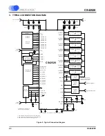
CS42528
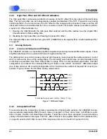
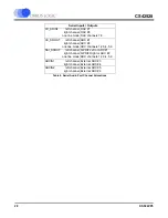
SWITCHING CHARACTERISTICS - CONTROL PORT - I
2
C FORMAT
(For CQZ, T
A
= -10 to +70° C; For DQZ, T
A
= -40 to +85° C; VA=VARX = 5 V, VD =VLS= 3.3 V; VLC = 1.8 V to 5.25 V; Inputs:
Logic 0 = DGND, Logic 1 = VLC, C
L
= 30 pF)
Notes: 16. Data must be held for sufficient time to bridge the transition time, t
fc
, of SCL.
17. The acknowledge delay is based on MCLK and can limit the maximum transaction speed.
18.
for Single-Speed Mode,
for Double-Speed Mode,
for Quad-Speed Mode
Parameter Symbol
Min
Max
Unit
SCL Clock Frequency
f
scl
-
100
kHz
RST Rising Edge to Start
t
irs
500
-
ns
Bus Free Time Between Transmissions
t
buf
4.7
-
µs
Start Condition Hold Time (prior to first clock pulse)
t
hdst
4.0
-
µs
Clock Low time
t
low
4.7
-
µs
Clock High Time
t
high
4.0
-
µs
Setup Time for Repeated Start Condition
t
sust
4.7
-
µs
SDA Hold Time from SCL Falling
(Note 16)
t
hdd
0
-
µs
SDA Setup time to SCL Rising
t
sud
250
-
ns
Rise Time of SCL and SDA
t
rc
-
1
µs
Fall Time SCL and SDA
t
fc
-
300
ns
Setup Time for Stop Condition
t
susp
4.7
-
µs
Acknowledge Delay from SCL Falling
(Note 17)
t
ack
-
(Note 18)
ns
15
256
Fs
×
---------------------
15
128
Fs
×
---------------------
15
64
Fs
×
------------------
t
b u f
t
h d s t
t
l o w
t
h d d
t
h ig h
t
su d
S to p
S t a r t
S D A
S C L
t
irs
R S T
t
h d st
t
rc
t
fc
t sust
t susp
S t a r t
S to p
R e p e a t e d
t
rd
t
fd
t
a c k
Figure 3. Control Port Timing - I
2
C Format