


- Lepton
9
- Technical Information Manual
20
style of transmission line, and its dimensions. The most common, and recommended PCB transmission line
scheme is to use a microstrip on the top or bottom layer of the PCB, with a ground plane on the layer
immediately adjacent as a return path. The width of this microstrip can then be varied to achieve the
desired characteristic impedance. Care should be taken to ensure that the microstrip trace has enough
current carrying capacity. This requires designing a trace that is heavy enough to withstand the heat
generated by power losses due to the resistance of the trace.
There are many online resources and tools designed to assist in designing PCB transmission lines with the
correct characteristic impedances. For example, the TXLine tool from National Instruments is very useful
for performing these calculations automatically. There is also an online calculator on eeweb.com. These
tools will require information about the PCB layout and also PCB characteristics, which should be obtained
from the PCB manufacturer.
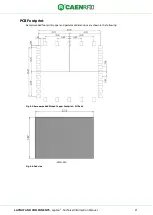
Package and Assembly Information
This section provides mechanical drawings and critical dimensions needed for PCB layout and housing
design, as well as SMT assembly information.
Package Mass
The mass of the Lepton
9
R9100C module is roughly 5.4 grams.
Package Dimensions
Package dimensions are shown in the following figure:
Fig. 4.2: Package Dimensions, Top, Front, and Side Views
Download the
Lepton
9
R9100C Technical drawing
Documents
section).