Caen V1729 Technical Information Manual Download Page 26


        PRELIMINARY


Document type: 

Title: 

Revision date: 

Revision: 

User's Manual (MUT) 

Mod. V1729 4 Channel 12 Bit Sampling ADC 

22/06/2005 


NPO: 

Filename: 

Number of pages: 

Page: 

00109/04:V1729.MUTx/03 V1729_REV3.DOC 

38 

26 


4.5.6 

Straps and resistor network sockets 


A certain number of sockets for straps and resistor networks are available on the board. 
These are their respective roles: 
 

Reference Role 

S1 

one utilizes the differential EXT_TRIG differential input (exclusive of S3) 

S3 

one utilizes the unipolar EXT_TRIG input by Lemo (exclusive of S1) 

S2 

the BUSY/SYNC_OUT output releases the BUSY signal (exclusive of S4) 

S4 

the BUSY/SYNC_OUT output releases the SYNC_OUT signal (exclusive of S2) 

S5 and S6  address of the board  

S7 

one utilizes the EXT_CLK input for the main clock (exclusive of S8)


S8 

one utilizes the 100MHz oscillator for the main clock (exclusive of S7)


S9 

Do not use


S10  

choice of the acquisition data bus


S11 

normally absent. Prevents the conf_done to rise which then permits not to 
validate the configuration of the Altera at power-up. 

S12 and 

S13 

address of the board


J3 

adaptation for the EXT_DIFF_TRIG input. Place 100 ohms between the pins 1 and 2 
and between the pins 3 and 4 

J4  

pull-down for the GPIB. Place an 8 resistor network 6.8k with common pin 

J5  

pull-up for the GPIB. Place an 8 resistor network 3.3k with common pin 

J6  

pull-down for the GPIB. Place an 8 resistor network 6.8k with common pin 

J7  

pull-up for the GPIB. Place an 8 resistor network 3.3k with common pin.  

Caution : only place these 4 networks once if the boards are linked.
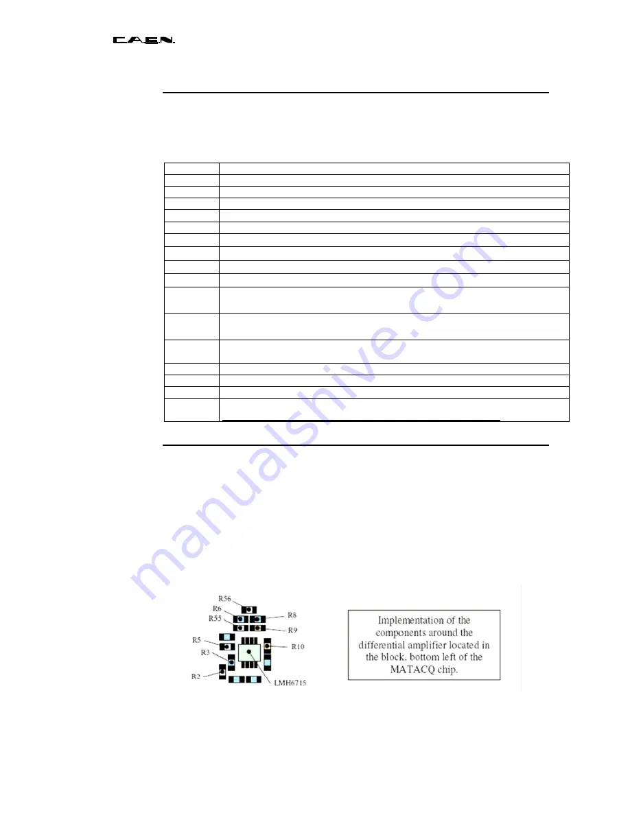
 

4.5.7 

Implementation of differential inputs 


The input signals are by default unipolar. In order to use differential inputs, one must 
make use of certain free CMS-805 resistor locations located close to the input amplifiers 
(LMH6715) and change some others. The equipment map of this zone of the board is 
presented below. The already present resistors appear in blue, whereas the free 
locations appear in white. 
In order to wire a differential input (with both inputs adapted on 50 ohms), one must first 
remove the resistors R3, R6 and R8. Then one has to put 84.5 ohms on R2, 0 ohm on 
R5 (use the former R3), 121 ohms on R55 and 50 ohms on R56. Finally, R9 (750 ohms) 
has to be replaced by 237 ohms and R10 (30.9 ohms) by 10 ohms. 


Summary of Contents for V1729

Page 1: ...Technical Information Manual MOD V1729 22 June 2005 Revision n 3 4 CHANNEL 12BIT SAMPLING ADC MANUAL REV 3 NPO 00109 04 V1729 MUTx 03...

Page 2: ...he User accident or any abnormal conditions or operations CAEN declines all responsibility for damages or injuries caused by an improper use of the Modules due to negligence on behalf of the User It i...

Page 3: ...NIZATION BETWEEN THE CHANNELS 16 3 1 1 Channels from the same board 16 3 1 2 Channels situated on different boards 16 3 2 SYNC_OUT AND BUSY SIGNALS 16 3 3 CALIBRATIONS 17 3 3 1 Calibration of the inte...

Page 4: ...ASES 7 FIG 2 3 SIMPLIFIED DESCRIPTION OF THE TRIGGER SELECTION CHAIN 9 FIG 2 4 SIMPLIFIED DESCRIPTION OF THE TRIGGER VALIDATION SYSTEM 10 FIG 2 5 BLOCK DIAGRAM OF A STANDARD ACQUISITION 12 FIG 2 6 TWO...

Page 5: ...al of a trigger signal initiates the stopping phase of the sampling 2 1 1 At the end of this phase the state of the memory is set it then contains the last 2560 points sampled of which 2520 are valid...

Page 6: ...not work properly with a pilot frequency Fp lower than 50MHz 1 3 Input signals Dynamic range The V1729 board integrates 4 analog channels The inputs of these channels are connected through double LEMO...

Page 7: ...of the stopping of the acquisition The POSTTRIG programmable by the user permits defining and displacing the position of the trigger signal in the acquisition window It is adjustable in the 1 Fp to 6...

Page 8: ...eral boards in order to produce at the exterior of the boards via their output TRIG_OUT a trigger which will be sent back to them in a synchronous way see figure 2 2 This mode is selected by the bit 4...

Page 9: ...signal which permits inhibiting the trigger as described on figure 3b is inhibited In order to perform the validation a programmable 8 bit latency counter called POST_STOP_LATENCY with steps of 2 5 s...

Page 10: ...his servo has to get locked again This implicates a typical waiting of 150 s before being able to reach the optimum of the sampling performances For this reason at each restarting of the acquisition t...

Page 11: ...nowledge the request by writing a 0 in the INTERRUPT register but the latter is anyhow reset by the START_ACQ command The first solution has the big advantage of being less noisy for the front end of...

Page 12: ...estal of a data cell is extremely reproducible 250 V RMS Due to the structure of the chip the dispersion of the pedestals presents a principal periodicity of 20 cells followed by a tiny individual dis...

Page 13: ...eration necessary for the treatment of the data is therefore to unfold the circular memory in order to obtain a table of 2560 temporally ordered data see Fig 2 6 This can be done by example by realizi...

Page 14: ...a jitter of a period of Fp The information of the 4 verniers from the same board being redundant in order to realize the temporal adjustement it is therefore possible to use solely the vernier from th...

Page 15: ...o 0 due to signal propagation times in the board of which the calibration is described in 3 1 1 An alternative but equivalent solution consists in generating the reordered table through a rotation tow...

Page 16: ...boards to generate the trigger signal on a fixed board master which triggers itself and to send its TRIG_OUT signal output to the external trigger input of the other boards via a NIM buffer if there...

Page 17: ...value on the left side MINVER will be the zero of the vernier and the one on the right side MAXVER will correspond to a vernier of 1 Fp in other words 10 or 20ns The intermediate values will next be d...

Page 18: ...n of the verniers The codes which implement the register setting is the following void TCAENADC Vernier char s 30 SetNCols 0 Setto PRETRIG SetPreTrig 1 Setto POSTTRIG SetPostTrig 1 SetTriggerType 0x08...

Page 19: ...vernier channel 0 vernier It is then necessary to rearrange the buffer in order to obtain 4 arrays one per channel of 16384 samples each With such settings we send on each channel a slope signal with...

Page 20: ...ither automatic or external The acquisition procedure is the same as for a standard acquisition but the reading of TRIG_REC can nevertheless be skipped Of course not the least temporal correction is m...

Page 21: ...oard by software which corresponds to a sampling frequency Fe 20 Fp of 1 or 2 GHz 4 3 Input signals Dynamic range The V1729 board integrates 4 analog channels The inputs of these channels are connecte...

Page 22: ...Filename Number of pages Page 00109 04 V1729 MUTx 03 V1729_REV3 DOC 38 22 4 4 Front panel Mod V1729 4 CH 12 BIT VCC EXT CLK ADC 8 TO 12 V 8 TO 12 V VME GPIB RESET CLOCK BUSY ACQRUNNING TRIG WR RAM IN...

Page 23: ...uration elements on the V1729 The V1729 board is of VME 6U mechanical format The two connectors P1 and P2 of the VME crate are usable both for the supply and the VME dialogue However these boards can...

Page 24: ...alf double LEMO I NIM EXT_TRIG External Trigger Half double LEMO I NIM EXT_DIFF_TRIG External Trigger Double pin I DIFF ECL EXT_CLK External clock LEMO I NIM TRIG_OUT Trigger Output LEMO O NIM BUSY SY...

Page 25: ...is dominant in relation to the time spent awaiting the event Y depends on the bandwidth mode 4 5 5 Pinout of the non standard connectors GPIB Connector HE10 26 points male Reference J2 1 D1 2 D5 3 D2...

Page 26: ...er up S12 and S13 address of the board J3 adaptation for the EXT_DIFF_TRIG input Place 100 ohms between the pins 1 and 2 and between the pins 3 and 4 J4 pull down for the GPIB Place an 8 resistor netw...

Page 27: ...ust be identical The range is saturated with 2k that is therefore the minimum value The tabulation below displays the different resistor values necessary to obtain the targeted shifts It is also neces...

Page 28: ...e same INTERRUPT register However it should be avoided because it is a source of noise during the data acquisition The reading of the data stored in the RAM is executed by realizing N successive readi...

Page 29: ...TERRUPT register Broadcast Mode A writing at the address 30 decimal permits realization of a writing in all the V1729 boards present on the GPIB bus 4 7 Reading of the data in the RAM mapping During t...

Page 30: ...ata The access to reading in the RAM is done by secondary addressing Its internal address is indeed controlled by a 16 bit counter RAM_INT_ADD located in the controller placed on the board in the FPGA...

Page 31: ...O 1C YES YES W Com SOFTWARE TRIGGER NO 0A YES NO W R Reg TRIGGER THRESHOLD DAC LSB byte GPIB 8 0 0B YES NO W R Reg TRIGGER THRESHOLD DAC MSB half byte GPIB 4 0 0A NO YES W R Reg TRIGGER THRESHOLD DAC...

Page 32: ...g is indirect the internal address of the RAM being defined by the RAM_INT_ADD counter located in the ALTERA RAM_INT_ADD this 16 bit counter fixes the internal address of the RAM for the bus access in...

Page 33: ...his 8 bit register gives the distance between the column where one finds the column pointer at the arrival time of the synchronous trigger and the last column 128 It permits in practice to roughly dat...

Page 34: ...xing of the Fp period It is initialized at 1 Bits Function 0 1 Val 1 Fsample 2GHz Val 2 Fsample 1GHz FPGA VERSION this 8 bit read only register permits reading of the version number of the FPGA The 3...

Page 35: ...ower readout of the MATACQ chips The management of writing and of re reading the digital memory RAM The interfacing with the acquisition system The last four blocks except the RAM itself as well as th...

Page 36: ...The elementary block of the analog acquisition is represented in Fig 4 4 It includes The 50 Ohm adaptation of the input A large bandwidth amplifier making it possible to feed the MATACQ chip in diffe...

Page 37: ...channel 15ps RMS typical Time precision between two channels 20ps RMS typical Depth per channel 2560 points of which 2520 are usable Trigger Threshold setting dynamic range 0 5V Threshold setting ste...

Page 38: ...6 2005 3 NPO Filename Number of pages Page 00109 04 V1729 MUTx 03 V1729_REV3 DOC 38 38 6 BIBLIOGRAPHY 1 E Delagnes D Breton Echantillonneur analogique rapide grande profondeur m moire French patent n...

Reviews: