III - 32
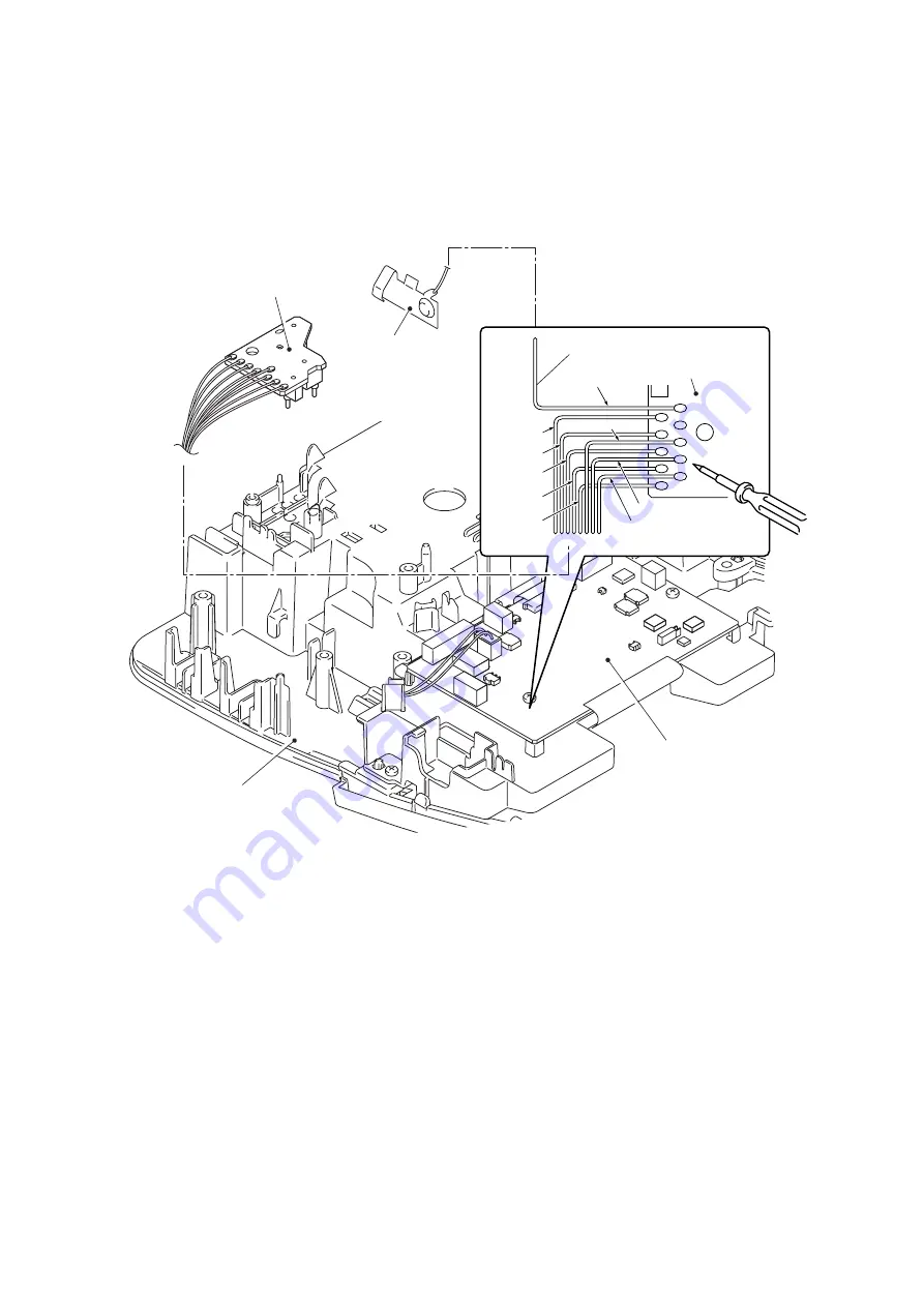
[ 6 ] Installing the Cassette PCB ASSY
CAUTION:
When handling the PCBs, put on the grounding wrist band. Failure to do
so might break LSIs and other electronic devices.
(1) Solder the eight cassette PCB leads and the battery terminal 2730 lead to the
main PCB ASSY.
Figure 3.1-36 Soldering the Leads
Cassette PCB ASSY
Battery terminal 2730
Battery terminal 2730 lead
Upper cover
Main PCB ASSY
Main PCB ASSY
Cassette PCB ASSY leads
(Yellow)
(White)
(Green)
(Yellow)
(Black)
(Brown)
(Red)
(Blue)
(Orange)
Summary of Contents for P-Touch PT-2730
Page 1: ...P touch SERVICE MANUAL MODEL PT 2730 ...
Page 7: ...I 3 Figure 1 1 2 Key Arrangement 1 PT 2730 USA ...
Page 8: ...I 4 Figure 1 1 3 Key Arrangement 2 PT 2730 UK ...
Page 9: ...I 5 Figure 1 1 4 Key Arrangement 3 PT 2730 DEU ...
Page 10: ...I 6 Figure 1 1 5 Key Arrangement 4 PT 2730 FRA ...
Page 78: ...III 58 Figure 3 3 27 Key Depressing Order ...
Page 84: ...III 64 3 4 Troubleshooting for the Test Mode 1 LCD Indication Check mode ...
Page 85: ...III 65 2 Cassette Sensor Switch Check mode ...
Page 86: ...III 66 ...
Page 87: ...III 67 3 Key Check mode ...
Page 88: ...III 68 4 Print Check mode 5 Cut Check mode ...
Page 89: ...III 69 ...
Page 90: ...III 70 6 Encode Reading Check mode ...
Page 93: ...IV 2 4 3 Troubleshooting Flows 1 Tape feeding failure ...
Page 94: ...IV 3 ...
Page 95: ...IV 4 2 Printing failure ...
Page 96: ...IV 5 ...
Page 97: ...IV 6 3 Powering failure Nothing appears on the LCD and the backlight does not light ...
Page 98: ...IV 7 ...
Page 99: ...IV 8 4 No key entry possible 5 Tape cutting failure ...
Page 100: ...IV 9 6 Interface port failure 7 LCD indication error or backlight error ...
Page 101: ...IV 10 8 Tape cassette type not identified ...
Page 102: ...A 1 APPENDIX 1 CIRCUIT DIAGRAMS Main PCB circuit diagram 1 2 ...
Page 103: ...A 2 Main PCB circuit diagram 2 2 ...
Page 104: ...A 3 Key PCB circuit diagram ...
Page 105: ...Sep 2010 SM PT037 ...


