background image


22 

Customize the embedded system based on


Your


Idea


configurations: 


7- or 8-bit data words, 1 or 2 stop bits, programmable parity (even, odd, or none) 


Programmable baud rates up to 4 Mbps. This is a higher max baud rate relative to the 1.875 MHz, 

which is stated by the TIA/EIA-232-F standard. 


32-byte FIFO on Tx and 32 half-word FIFO on Rx supporting auto-baud 

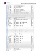
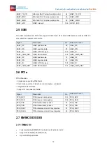
Signal 

Description 

Pin 

Defaults Function 

UART1_CTS_B 

UART1 clear to send 

16 

UART3_RXD 

UART1_RTS_B 

UART1 request to send 

171 

UART3_TXD 

UART1_RXD 

UART1 data input 

156 

UART1_RXD   

UART1_TXD 

UART1 data output 

154 

UART1_TXD 

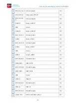
UART2_CTS_B 

UART2 clear to send 

144 

UART4_RXD 

182 

SAI3_RXC 

UART2_RTS_B 

UART2 request to send 

142 

UART4_TXD 

181 

SAI3_RXD 

UART2_RXD 

UART2 data input 

152 

UART2_RXD 

185 

SAI3_TXFS 

UART2_TXD 

UART2 data output 

150 

UART2_TXD 

179 

SAI3_TXC 

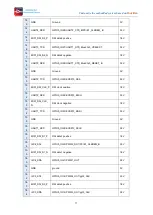
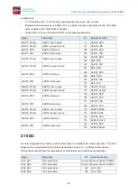
UART3_CTS_B 

UART3 clear to send 

173 

UART3_CTS_B 

UART3_RTS_B 

UART3 request to send 

175 

UART3_RTS_B 

UART3_RXD 

UART3 data input 

169 

UART3_RXD 

148 

UART1_CTS 

UART3_TXD 

UART3 data output 

171 

UART3_TXD 

146 

UART1_RTS 

UART4_CTS_B 

UART4 clear to send 

172 

ECSPI2_MISO 

UART4_RTS_B 

UART4 request to send 

176 

ECSPI2_SS0 

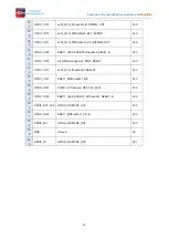
UART4_RXD 

UART4 data input 

144 

UART4_RXD 

174 

ECSPI2_SCLK 

UART4_TXD 

UART4 data output 

142 

UART4_RXD 

170 

ECSPI2_MOSI 

2.10 I2C 

The Inter-Integrated Circuit (I2C) provides functionality of a standard I2C master and slave. The I2C is 

designed to be compatible with the I2C Bus Specification, version 2.1, by Philips Semiconductor. 

I2C provides serial interface for external devices. Data rates of up to 320 kbps are supported. 

Signal 

Description 

Pin 

Defaults Function 

I2C1_SCL 

I2C1 serial clock   

Un-pinout  Communication t0 PMIC 

I2C1_SDA 

I2C1 serial data 

Un-pinout  Communication t0 PMIC 

I2C2_SCL 

I2C2 serial clock   

166 

I2C2_SCL 

I2C2_SDA 

I2C2 serial data 

168 

I2C2_SDA 

Summary of Contents for PICO-IMX8M-MINI

Page 1: ...PICO IMX8M MINI Reference User Manual V1 202003 www boardcon com Boardcon Embedded Design...

Page 2: ...Warranty Boardcon warrants this product to be free of defects in material and workmanship for a period of one year from date of buy During this warranty period Boardcon will repair or replace the defe...

Page 3: ...M MINI 14 2 Peripheral Introduction 15 2 1 Display 15 2 2 Camera I F 15 2 3 Audio 16 2 3 1 Digital Interface SAI 16 2 3 2 Sony Philips Digital Interface 18 2 4 Ethernet 18 2 5 USB 19 2 6 PCIe 19 2 7 E...

Page 4: ...dvertising machine new retail vending ticketing machine human computer interactive query and business processing machine high performance instruments industrial and medical industrial control and huma...

Page 5: ...integrated PHY PCIe 1x PCIe 2 0 1 lane with L1 low power substates Ethernet RGMII interface Temperature 0 C to 70 C 1 3 SoM Specifications Feature Specifications CPU NXP i MX8M Mini 4x Cortex A53 cor...

Page 6: ...y TrustZone DRM Ciphers Secure Clock eFuse Key Storage Random Number 32 KB Secure RAM Main CPU Platform Quad Cortex A53 32 KB I cache 32 KB D cache NEON FPU 512 KB L2 Cache Cortex M4 16 KB I cache 16...

Page 7: ...RT EXP CN LPDDR4 DRAM x bi 32 ts eMMC 5 1 x s 8 bit GPIO SAI I2C GPI T O UAR Au d dio Car SAI GPIO I2C MicroSD Button ONOFF x s 4 bit SDIO SDIO ONOF PIO F G JTAG MIPI DSI MIPI CSI SDIO UART PCM PCIe S...

Page 8: ...TXD7 GPIO4_IO19 SAI6_MCLK with pull D 4 7K 3 3V 28 SAI1_TXD6 GPIO4_IO18 SAI6_RxSYNC pull Down 10K 3 3V 29 SAI1_TXD5 GPIO4_IO17 SAI6_RxData0 pull Up 10K 3 3V 30 SAI1_TXD4 GPIO4_IO16 SAI6_RxBCLK pull D...

Page 9: ...3 3V 64 ENET_TX_CTL GPIO1_IO22 ENET1_RGMII_TX_CTL 3 3V 65 GND ground 0V 66 ENET_TD0 GPIO1_IO21 ENET1_RGMII_TD0 3 3V 67 ENET_TD1 GPIO1_IO20 ENET1_RGMII_TD1 3 3V 68 ENET_TD2 GPIO1_IO19 ENET1_RGMII_TD2 I...

Page 10: ...usdhc2_DATA1 3 3V 10 3 PCIE_RXN_P PCIE input positive 1 8V 10 4 SD2_DATA2 GPIO2_IO17 usdhc2_DATA2 3 3V 10 5 PCIE_RXN_N PCIE input negative 1 8V 10 6 SD2_DATA3 GPIO2_IO18 usdhc2_DATA3 3 3V 10 7 GND GN...

Page 11: ...1 8 V 12 8 CLKIN1 anamix_CLKIN1 1 8V 12 9 MIPI_CSI_D1_N CSI data1 negative 1 8V 13 0 CLKIN2 anamix_CLKIN2 1 8V 13 1 GND Ground 0V 13 2 ONOFF snvsmix_ONOFF 1 8V 13 3 MIPI_CSI_D0_P CSI data0 positive 1...

Page 12: ...SS0 3 3V 15 1 MIPI_DSI_CLK_P DSI clock positive 1 8V 15 2 UART2_RXD GPIO5_IO24 ECSPI3_MISO 3 3V 15 3 MIPI_DSI_CLK_ N DSI clock negative 1 8V 15 4 UART1_TXD GPIO5_IO23 ECSPI3_MOSI 3 3V 15 5 GND Ground...

Page 13: ...7 4 ECSPI2_SCLK GPIO5_IO10 UART4_RX 3 3V 17 5 ECSPI1_SS0 GPIO5_IO9 UART3_RTS_B 3 3V 17 6 ECSPI2_SS0 GPIO5_IO13 UART4_RTS_B 3 3V 17 7 GND Ground 0V 17 8 SAI3_TXD GPIO5_IO1 SAI3_TX_Data0 SAI5_RxData3 3...

Page 14: ...dhc2_RESET_B 3 3V 19 1 GPIO1_IO05 m4 NMI ccmsrcgpcmix_PMIC_READY 3 3V 19 2 GPIO1_IO11 usb2_OTG_ID usdhc3_VSELECT 3 3V 19 3 GPIO1_IO07 ENET1_MDIO usdhc1_WP 3 3V 19 4 GPIO1_IO01 PWM1_OUT anamix_REF_CLK_...

Page 15: ...tek RTL8211E Audio WM8960 audio codec 3 5mm audio jack 2x 2pin header for Speaker Expand Audio 8bit RX and 8bit TX SAI interface 40 pin header J5 SD Micro SD socket SD3 01 Display MIPI DSI 4 data lane...

Page 16: ...sed for SAI1_RXFS 2 1 Display MIPI DSI Features 4 lane MIPI DSI up to 1920 x 1080 60Hz Touchscreen capacitive touch screen support through I2C interfaces Up to a maximum bit rate of 1 5 Gbps Signal De...

Page 17: ...hronous audio interface SAI modules supporting I2S AC97 TDM codec DSP and DSD interfaces including one SAI with 8 Tx and 8 Rx lanes one SAI with 4 Tx and 4 Rx lanes two SAI with 2 Tx and 2 Rx lanes an...

Page 18: ...7 SAI3_RXD SAI3 Receive data 181 SAI3_RXD SAI3_RXC SAI3 Receive bit clock 183 SAI3_RXC SAI3_RXFS SAI3 Receive frame sync 185 SAI3_RXFS SAI3_TXD SAI3 Transmit data 178 SAI3_TXD SAI3_TXC SAI3 Transmit b...

Page 19: ...PDIF_EXT_CLK 2 4 Ethernet The Ethernet Media Access Controller MAC is designed to support 10 100 1000 Mbps Ethernet IEEE 802 3 networks Used PHY chip RTL8211E VB CG Features 1000Base T IEEE 802 3ab Co...

Page 20: ...ta 79 USB2_DP USB2_DN USB2 negative data 81 USB2_DN USB2_ID USB2 OTG ID signal 138 USB2_ID USB2_VBUS_DET USB1 VBUS detect 134 USB2_VBUS_DET 2 6 PCIe PCI E Features Single lane supporting PCIe Gen2 Dua...

Page 21: ...signals Signal Description Pin Defaults Function SD2_DATA0 SDIO2 data0 100 SD2_DATA0 SD2_DATA1 SDIO2 data1 102 SD2_DATA1 SD2_DATA2 SDIO2 data2 104 SD2_DATA2 SD2_DATA3 SDIO2 data3 106 SD2_DATA3 SD2_nC...

Page 22: ...input Master data output 152 UART2_RXD ECSPI3_SS0 SPI3 Chip Select0 150 UART2_TXD 2 8 2 QSPI Signal Description Pin Defaults Function QSPIA_SCLK SPIA Master clock put out Un pinout QSPIA_SCLK for flas...

Page 23: ...T2_TXD 179 SAI3_TXC UART3_CTS_B UART3 clear to send 173 UART3_CTS_B UART3_RTS_B UART3 request to send 175 UART3_RTS_B UART3_RXD UART3 data input 169 UART3_RXD 148 UART1_CTS UART3_TXD UART3 data output...

Page 24: ...IFO to generate sound Signal Description Pin Defaults Function PWM1 PWM1 output 194 GPIO1_IO01 196 SPDIF_EXT_CLK 160 I2C4_SDA PWM2 PWM2 output 184 GPIO1_IO13 198 SPDIF_RX 158 I2C4_SCL PWM3 PWM3 output...

Page 25: ...3 5 3 3 3 3 5 V Isys_in VSYS input Current 800 1500 mA Ivio_out VCC_IO output Current 1000 1200 mA VCC_RTC RTC Voltage 1 8 3 3 4 V Iirtc RTC input Current 5 7 uA Ta Operating Temperature 0 70 C Tstg...

Reviews: