Wide input / output, Buck-boost, ±Output DC/DC Converter
1 Watt BUD Series
9
Bellnix
DC-DC Converter
BDD20200930_Z02(BDD20190924_Z02)
7. How to use
7-1. Standard connection diagram and recommended layout
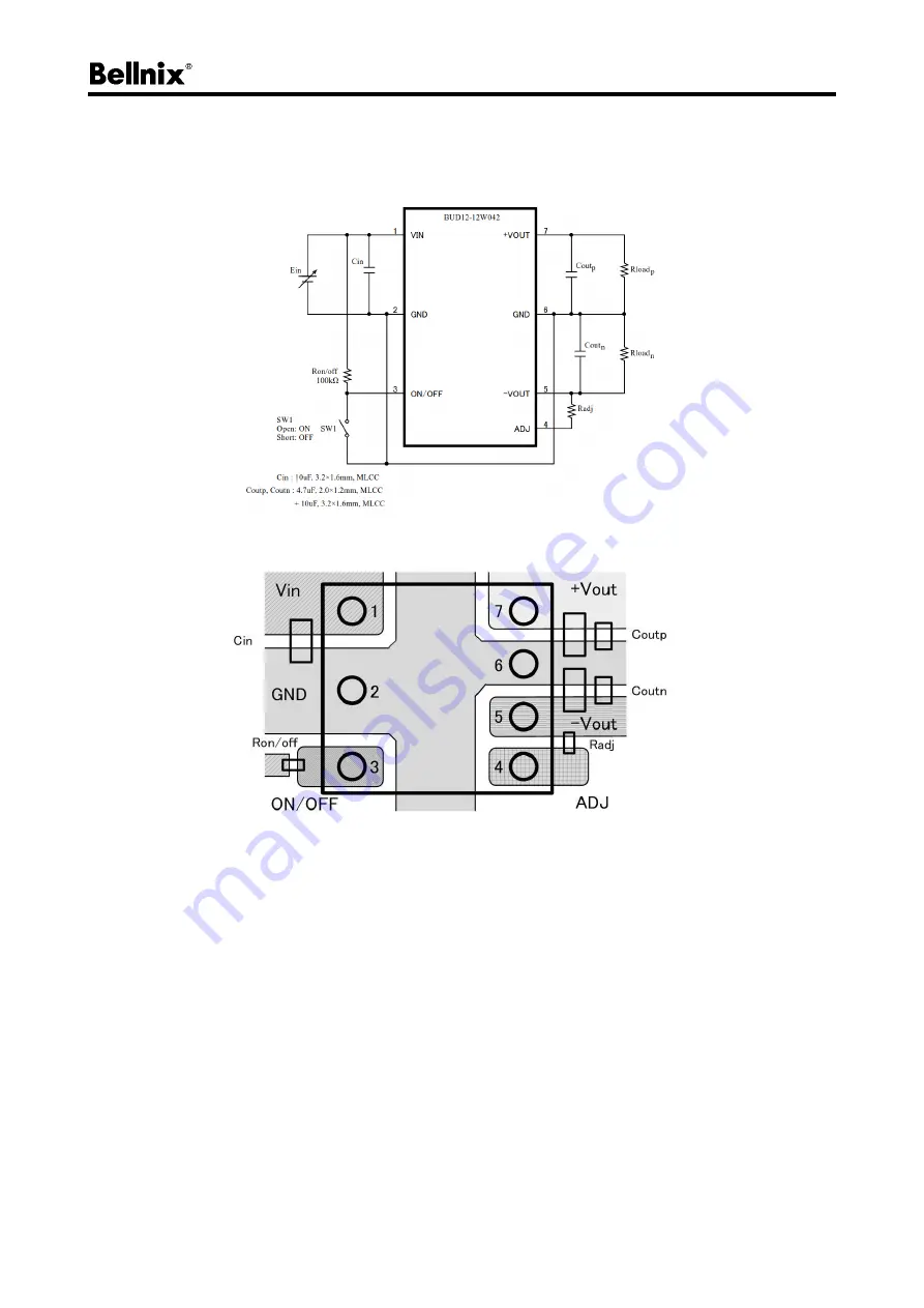
Standard connection diagram
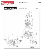
Recommended layout
Note 1: Radj is the output voltage setting resistor. Be sure to connect a resistor with a value according to
the output voltage setting (Section 7-2), and do not leave it OPEN.
Note 2: Connect the input and output capacitors Cin, Cout
p
, Cout
n
as close as possible to the converter pin.
Note 3: The recommended layout diagram shows only the mounting surface. Design the pattern in
consideration of the input and output conditions and the ambient temperature to be used.
Note 4: If the output load is less than 0.05W on one side, the regulation rate may increase depending on the
conditions.


