Atmel AVR910 Application Note Download Page 5

5

0943E–AVR–08/08

AVR910

SCK pin stable, as one single edge will cause the target to loose synchronization with the pro-
grammer. For other devices use the synchronization algorithm specified in the datasheet. After
pulling Reset low, wait at least 20 ms before issuing the first command.

Command Format

All commands have a common format consisting of four bytes. The first byte contains the com-
mand code, selecting operation and target memory. The second and third byte contain the
address of the selected memory area. The fourth byte contains the data, going in either
direction.

The data returned from the target is usually the data sent in the previous byte. Table 3 shows an
example, where two consecutive commands are sent to the target. Notice how all bytes returned
equal the bytes just received. Some commands return one byte from the target’s memory. This
byte is always returned in the last byte (byte 4). Data is alwa‘ys sent on MOSI and MISO lines
with most significant bit (MSB) first.

For details on available instructions, please refer to the Serial Programming section of the
datasheet.

Enable Memory 
Access

When the Reset pin is first pulled active, the only instruction accepted by the SPI interface is
“Programming Enable”. Only this command will open for access to the Flash and EEPROM
memories, and without this access, any other command issued will be ignored. Table 3 shows
an example where memory access is enabled in the first command sent to the chip.

After a “Programming Enable” command has been sent to the target, access is given to the non-
volatile memories of the chip according to the current setting of the protecting Lock bits.

The target AVR microcontroller will not respond with an acknowledge to the “Programming
Enable” command. To check if the command has been accepted by the target AVR microcon-
troller, the device code could be read. The device code is also known as the signature bytes.

Device Code

After the “Programming Enable” command has been successfully read by the SPI interface, the
programmer can read the device code. The device code will identify the chip vendor (Atmel), the
part family (AVR), Flash size in kilobytes, and family member (i.e., AT90S1200). The “Read
Device Code” command format is found in the Serial Programming section of the datasheet. As
an example, this command will, for the AT90S1200, be [$30, $XX, $adr, $code]. Valid addresses
are $00, $01 and $02. Table 4 shows what the expected result will be.

.

Table 5 indicates that Device Code will sometimes read as $FF. If this happens, the part device
code has not been programmed into the device. This does not indicate an error, but the part has
to be manually identified to the programmer.

Device code $FF might also occur if there is no target ready or if the MISO line is constantly
pulled high. The programmer can detect this situation by detecting that also a command sent to
the target is returned as $FF. 

If the target reports Vendor Code $00, Part Family $01, and Part Number $02, both Lock bits
have been set. This prevents the memory blocks from responding, and the valued returned will
be the byte just received from the programmer, which just happens to be the current address. To
erase the Lock bits, it is necessary to perform a valid “Chip Erase”.

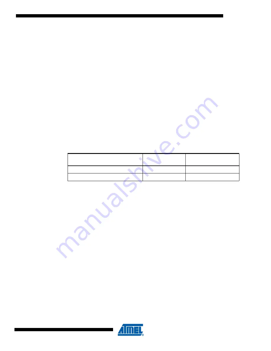
Table 3.  Example, Enabling Memory Access and Erasing the Chip

Action

MOSI, Sent to 

Target AVR

MISO, Returned from 

Target AVR

Programming Enable

$AC 53 xx yy

$zz AC 53 xx

Read Device Code $1E at Address $00

$30 nn 00 mm

$yy 30 nn 1E

Summary of Contents for AVR910

Page 1: ...target AVR microcontroller to be programmed from any PC equipped with a regular 9 pin serial port Alternatively the entire In System Programmer can be built into the system allowing it to reprogram itself The Programming Interface For In System Programming the programmer is connected to the target using as few wires as possible To program any AVR microcontroller in any target system a simple Six w...

Page 2: ...Connector Layout Top View Hardware Design Considerations To allow In System Programming of the AVR microcontroller the In System Programmer must be able to override the pin functionality during programming This section describes the details of each pin used for the programming operation GND The In System Programmer and target system need to operate with the same reference voltage This is done by c...

Page 3: ...did not echo back give Reset a positive pulse and issue a new Programming Enable command Note that all four bytes of the of the Programming Enable command must be sent before starting a new transmission The target AVR microcontroller will always set up its SCK pin to be an input with no pull up whenever Reset is active See also the description of the Reset wire Table 1 Connections Required for In ...

Page 4: ...e its power supplied from the programmer through the same connector used for the communication This would allow the target to be programmed without applying power to the target externally Programming Protocol Immediately after Reset goes active on the target AVR microcontroller the chip is ready to enter Programming mode The internal Serial Peripheral Interface SPI is activated and is ready to acc...

Page 5: ... the protecting Lock bits The target AVR microcontroller will not respond with an acknowledge to the Programming Enable command To check if the command has been accepted by the target AVR microcon troller the device code could be read The device code is also known as the signature bytes Device Code After the Programming Enable command has been successfully read by the SPI interface the programmer ...

Page 6: ...or high byte with the H bit in the command byte 0 is low 1 is high byte The byte stored at this address is then returned from the target AVR microcontroller in byte 4 Usually each 16 bit word in Flash contains one AVR instruction Assuming the instruction stored at address 104 is add r16 r17 the op code for this instruction would be stored as 0F01 Reading address 104 serially the expected result re...

Page 7: ...e devices there is no method to detect when the Flash write cycle has ended For this reason the programmer presented in this application note waits N ms before attempting to send another command to the interface the delay N will depend on target device and can be found in the programming section of the datasheet For some devices it is possible to use polling When a byte is being programmed into th...

Page 8: ...tected from further writing or you may completely disable both reading and writing of memories on the chip In some devices the Lock bits can not be read and setting Lock bits can not be verified by the programmer To check that the Lock bits have been set properly in these devices one should attempt to alter a location in EEPROM When Lock bit 1 is set memory locations are not altered When both Lock...

Page 9: ... setting a bit to one Erasing the memory is performed with the Chip Erase command This command will erase all memory contents both Flash Program Memory and EEPROM Only after a successful erase of the memory the Lock bits will be erased This method ensures that data in the memories are kept secured until all data have been completely erased After a Chip Erase all memory contents will be read as FF ...

Page 10: ...tive line voltage The transmit line is fed with this negative voltage from C100 when transistor Q100 is closed This sends a logical one on the transmit line Logical zeros positive voltage is sent by opening Q100 connecting VCC actually VCC 0 2V to the transmit line Some older PC systems might have serial port not accepting voltages below 10 volts as logical zero This however is not a problem with ...

Page 11: ... 6 PIN HEADER IDC FEMALE CABLE MOUNT 1 Q100 45V 100MA BC857C PHILIPS SMD NPN TRANSISTOR SO 23 PACKAGE 1 Q101 45V 100MA BC847C PHILIPS SMD PNP TRANSISTOR SO 23 PACKAGE 6 R100 105 4K7 R08_4K7 1 KOA RESISTOR 0 125W 1 0805 1 R106 1M0 NOT_USED 1 KOA RESISTOR 0 125W 1 0805 1 U100 SOIC 20 AT90S1200 4SC ATMEL AVR MICROCONTROLLER 20 PIN SOIC 1 XC100 4 0MHZ CSTCC4 00MG 0 5 MURATA AVX CERAMIC RESONATOR 4 00 ...

Page 12: ...OR STATUTORY WARRANTY RELATING TO ITS PRODUCTS INCLUDING BUT NOT LIMITED TO THE IMPLIED WARRANTY OF MERCHANTABILITY FITNESS FOR A PARTICULAR PURPOSE OR NON INFRINGEMENT IN NO EVENT SHALL ATMEL BE LIABLE FOR ANY DIRECT INDIRECT CONSEQUENTIAL PUNITIVE SPECIAL OR INCIDEN TAL DAMAGES INCLUDING WITHOUT LIMITATION DAMAGES FOR LOSS OF PROFITS BUSINESS INTERRUPTION OR LOSS OF INFORMATION ARISING OUT OF TH...

Reviews: