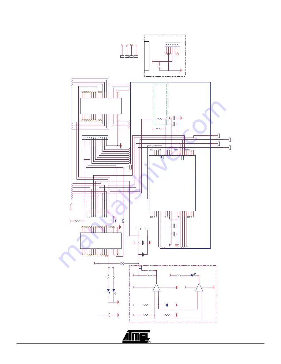
Atmel ATEVK525 Hardware User'S Manual Download Page 26

Complete Schematics

7-26

ATEVK525 Mass Storage Board for AVR

7740B–AVR–03/08

Figure 7-1 .  

Schematics, 1 of 1

NC1

1

NC2

2

NC3

3

NC4

4

NC5

5

NC6

6

R/B

7

RE

8

CE

9

NC7

10

NC8

11

VCC1

12

VSS1

13

NC9

14

NC10

15

CLE

16

ALE

17

WE

18

WP

19

NC11

20

NC12

21

NC13

22

NC14

23

NC15

24

NC16

25

NC17

26

NC18

27

NC19

28

I/O0

29

I/O1

30

I/O2

31

I/O3

32

NC20

33

NC21

34

NC22

35

NC29

48

NC28

47

NC27

46

NC26

45

I/O7

44

I/O6

43

I/O5

42

I/O4

41

NC25

40

NC24

39

NC23

38

VCC2

37

VSS2

36

48 PINS WS

OP

x8 NAN

D FLASH 

U3

MT29F2G08AACWP


VSRC

R1

47k

VCC

NF_nWP0NF_nWP0NF_nWP0NF_nWP0NF_nWP0NF_nWP0NF_nWP0NF_nWP0

NF_R/nB0NF_R/nB0NF_R/nB0NF_R/nB0NF_R/nB0NF_R/nB0NF_R/nB0NF_R/nB0NF_R/nB0NF_R/nB0NF_R/nB0NF_R/nB0

VSRC

VSRC

PA5

PA0

PA4

PA6

PA3

PA7

PA2

PA1

1

TP7

NF_ALE

VSRC

1

TP10

GND

3

2

1

8

4

-

+

U1A

LM393/SO

OPTIONAL

Overvoltage

Protection

Circuit

Decoupling cap

acitor

must be near t

o IC

5

6

7

8

4

-

+

U1B

LM393/SO

Decoupling capacitor

must be ne

ar to IC

Decoupling capac

itor

must be 

near to 

IC

R2

820

R3

820

Q1

Si2301

1

TP2

SD_MISO

D1

HSMC-C170

WRITE

VSRC

D2

HSMG-C170

READ

VCC

SO

SCK

SI

1

3

2

4

5

6

7

SD/MMC

J5

nCS_mmc

SD/MMC CONNECTOR

VCC

Unsolder R8 and R10 resistor

if optio

nal NAND Flash

module is m

ounted !

NF_nRENF_nRENF_nRENF_nRE

NF_R/nB1NF_R/nB1NF_R/nB1NF_R/nB1NF_R/nB1NF_R/nB1NF_R/nB1NF_R/nB1NF_R/nB1NF_R/nB1NF_R/nB1NF_R/nB1NF_R/nB1NF_R/nB1NF_R/nB1NF_R/nB1NF_R/nB1NF_R/nB1NF_R/nB1NF_R/nB1NF_R/nB1NF_R/nB1

NF_nCE1

R8

0

NF_nWENF_nWENF_nWENF_nWENF_nWENF_nWENF_nWENF_nWE

R4

150k

VCC

10 nF


C3

PA0

NF_D2

1nF


C4

PA3

NF_D3

PA2

PA4

NF_D4

NF_D5

PA5

PA7

PA6

SO

NF_D7

PA1

1

TP3

SD_SCK

PA3

SCK

NF_nWP3

NF_nWENF_nWE

PA5

CP2

NF_nWP1

R9

75k

PA7

SI

NF_nRE

PC[7..0]

PC3

PC7

CP1

PC1

PC6

PC0

NF_nCE0

PC2

1

TP9

NF_RE

PC0PC0

VCC

PA0

R5

47k

NF_nCE2

PC4

NF_D0

NF_D1

PA1

PC5

PA2

R6

10k

PC3 
PC2

NF_nCE3

PA4

PA6

NF_D6

PC4

PC5

PC1

NF_R/nB2

R11

47k

PA[7..0]

PC7 
PC6

NF_R/nB3

VCC

1

TP4

SD_MOSI

GND

1

GND

2

AUXI1

3

AUXO1

4

DATA7

5

DATA6

6

DATA5

7

DATA4

8

DATA3

9

DATA0

10

DATA1

11

DATA9

12

SI

13

SO

14

SCK

15

CS

16

XT1

17

XT2

18

VTG

19

VTG

20

GND

21

GND

22

PB7

23

PB6

24

PB5

25

PB4

26

PB3

27

PB2

28

PB1

29

PB0

30

PD7

31

PD6

32

PD5

33

PD4

34

PD3

35

PD2

36

PD1

37

PD0

38

GND

39

GND

40

CON 2x20

J1

EXP. CON 

1

R7

47k

10 nF


C6

1nF

C5

GND

1

GND

2

AUXI0

3

AUXO0

4

CT7

5

CT6

6

CT5

7

CT4

8

CT3

9

CT2

10

CT1

11

BSEL2

12

(n.c.)

13

REF

14

NRST

15

PE2

16

PE1

17

PE0

18

GND

19

GND

20

VTG

21

VTG

22

PC7

23

PC6

24

PC5

25

PC4

26

PC3

27

PC2

28

PC1

29

PC0

30

PA7

31

PA6

32

PA5

33

PA4

34

PA3

35

PA2

36

PA1

37

PA0

38

GND

39

GND

40

CON 2x20

J3

EXP. CON 

0

SP1

1

2

3

4

5

6

7

8

9

10

11

12

13

J4-NF_CON#2

NF MODULE

1

2

3

4

5

6

7

8

9

10

11

12

13

J2-NF_CON#1

NF MODULE

VCC

NF_CLE

C2

4,7µF

R10

0

D3

HSML-C170

PWR FAIL

1

TP5

SD_CS

1

TP6

NF_CLE

NF_ALE

NF_nWP2

R12

820

VSRC

SO

2

1

U2

LM385-1,2/SOT23

C8

4,7µF

SCK

1

TP1

VCC

10 nF


C7

nCS_mmc

SI

C1

1µF

1

TP8

NF_WE

VSRC

nCS_mmc

Summary of Contents for ATEVK525

Page 1: ...ATEVK525 Mass Storage Board for AVR Hardware User Guide ...

Page 2: ... 7 2 3 SD MMC Card 2 11 2 4 LEDs 2 12 2 5 Test Points 2 12 2 6 Configuration Pads 2 13 2 7 Solder Pads 2 14 Section 3 Software Implementation 3 15 3 1 Software packages 3 15 3 2 Performances 3 17 3 3 Driver limitations 3 18 3 4 Usage Notes 3 19 3 5 Handling another NAND Flash device 3 19 Section 4 Troubleshooting Guide 4 21 Section 5 Technical Specifications 5 23 Section 6 Technical Support 6 24 S...

Page 3: ...SBxxx Generic Product Name microcontroller This board is designed to allow an easy evaluation of USB Mass Storage using demonstration software The ATEVK525 board has been designed to be plugged into the Atmel STK525 Starter Kit Board in order to add Mass Storage capability to an existing development board and to combine them with other features USB RS232 Microphone but also all AVR development too...

Page 4: ...wing features NAND Flash chip soldered Micron MT29F2G08AACWP 256 MBytes Reserved location additional NAND Flash chips module plug in Receptacle for SD and MMC memory cards LED signalling for Read Write operations Power supply 3 3V regulated from motherboard Additional overvoltage protection circuitry optional with failure indicator Numerous access points for debug ...

Page 5: ...25 is an extension board that must be plugged on another microcontroller hosting board like STK525 AT90USBxxx support that provides supply voltage Figure 2 1 Connecting the ATEVK525 under the STK525 Note The ATEVK525 can also be plugged onto the STK525 but in this configuration the user must take care to avoid contact between the board and either the JTAG plug or the microcontroller ZIF socket ...

Page 6: ...icrocontroller I O levels and this voltage must be present on the VTG pins of the EXPAND connectors On the STK525 the configuration must be JP4 closed ties 3 3V to VTG pins VCC SOURCE set to REG 3 3 mode powers microcontroller I O at 3 3V Figure 2 2 Configuration to set on STK525 NAND Flash MT29F2G08AACWP current consumption is 1mA maximum in idle state and can reach 30mA 15mA typ during access op...

Page 7: ...ect power supply of the on board resources see photo above 2 2 NAND Flash 2 2 1 Default device The ATEVK525 comes with one NAND Flash chip soldered At the time of writing this chip is the Micron MT29F2G08AACWP that features 2 GBits 256 MBytes organized as 2048 blocks block size 64 pages page size 2112 bytes 2048 64 in spare zone Page program time of 300µs Block erase time of 2ms Copy Back feature ...

Page 8: ...cle footprints 2 54mm pitch Users can solder a receptacle on the board and then insert a NAND Flash module described below or directly solder the module Figure 2 4 NAND Flash module example Table 2 2 NAND Flash module pin out description NAND Flash Microcontroller Function I O 7 0 PORTA 7 0 A7 A0 Data and Address bus CLE PORTC0 A8 Command Latch Enable ALE PORTC1 A9 Data Latch Enable RE PORTE1 RD R...

Page 9: ... and mount devices on this board BOM and components placement Each module can receive up to four different devices according to the following placement Table 2 3 NAND Flash devices placement 4 WP0 4 WP1 5 VCC 5 D7 6 CLE 6 D6 7 ALE 7 D5 8 R B1 8 D4 9 CE0 9 D3 10 R B0 10 D2 11 CE1 11 D1 12 RE 12 D0 13 WE 13 GND NFCON1 NFCON2 Pin Function Pin Function ...

Page 10: ...dule 2 When using the additional module check that the configuration pads that enable CTS RTS lines on STK525 are not soldered because these signals are also con nected to the R B 2 3 But if CTS RTS lines are required you cannot use the R B 2 3 signals so disable the configuration pads CP1 CP2 of the ATEVK525 NAND Flash Microcontroller Function CE0 PORTC2 A10 Chip select for chip 0 active low on b...

Page 11: ...fert speed but is easy to implement The alternate access method is a parallel mode Command set cards have numerous commands that are common enough to completely control the memory Only the initialization process is different but a standard procedure automatically enables card identification and initialization Be aware of the card specification version information contained in the CSD structure of ...

Page 12: ...when initiating a SCSI Read command Figure 2 7 On board SCSI signalling LEDs 2 5 Test Points Several test points are included on the board to facilitate debug during development All the test points are circular pads with a silk screen printing that indicates the corresponding signal VCC power supply voltage should be 3 3V taken after the power protection circuit GND power supply ground SD_MISO SD ...

Page 13: ... Note See section 2 2 2 Additional devices for more details 2 6 2 Configuration Pads Disconnection Figure 1 Configuration Pad Disconnection 2 6 3 Configuration Pads Connection Figure 2 Configuration Pad Re connection Config Pads Reference Related Signals Function CP1 R nB2 Connect Ready notBusy signal from NF 2 third NF of the optionnal module to STK525 CP2 R nB3 Connect Ready notBusy signal from ...

Page 14: ...oard peripherals or elements Their default configuration is disconnect User may solder the pad to enable it 2 7 1 Solder Pads Listing Table 2 7 Solder Pads Solder Pads Reference Related Signals Function SP1 VCC This solder pad allows power protection circuit bypassing If this optional circuit is not mounted this solder pad must be soldered ...

Page 15: ...sh 8 MB disk This package can be found on the CD ROM provided with the kit USB Dual Role Host Device with FAT support and Shell 1 In Device mode B connector plugged the package is identical to the first package that enumerates three hardware storage volumes through the USB 2 In Host mode A connector plugged the application allows connecting one USB mass storage device 3 In both modes the STK525 ca...

Page 16: ...back to previous directory mount disk mount drive a b mkdir filename create a directory disk get number of drives and memory type associated goto goto bookmark df get free space information rm delete all files in the directory lsusb get information about the connected device in host mode only suspend suspend USB bus activity resume resume USB bus activity reboot reset the aplication This package i...

Page 17: ...size limited zones This problem con cern several other memorie devices 3 2 2 Direct limitations The limitations on reading operations are Dataflash SPI bus frequency internal read access speed SD MMC SPI bus frequency internal read access speed NAND Flash USB maximum data rate The limitations on writing operations are Dataflash internal write access speed page write duration size SPI bus frequency...

Page 18: ...ns in a software way or by implementing SD Bus operation in a more hardware way 3 3 3 NAND Flash The NAND Flash technology and the consumer request for continually faster and larger devices conduce to numerous enhancements of memories structure and thus memory management drivers Limitations The COPYBACK feature is not address dependent in the current driver version This means that the instruction ...

Page 19: ... be updated in the memory all the corresponding blocks each block contains 64 pages for example is copied to a new free block and the required page is modified during the copy To end this operation of block translation all the pages up to the modified one are programmed But to precede an optional contiguous write operation the pages that end the block the block tail are not yet programmed They wil...

Page 20: ...you must define the memory name For example the board comes with the default configuration define NF_TYPE_MT29F2G08AACWP if you want to use different modules with different memory references without modifying the driver you must enable to TRUE either NF_AUTO_DETECT_2KB or NF_AUTO_DETECT_512B according to the page size of the memory ...

Page 21: ...thing for the JTAG plug if used Protection circuit problem If the PWR_FAIL LED is lighting ON whereas the voltage you measure on VCC is correct bypass the protection circuitry solder SP1 NAND Flash device onboard chip only does not work Additional module is mounted The onboard memory chip cannot be accessed while the optional NAND Flash module is mounted since two memories will share their chip se...

Page 22: ...oes not work Bad physical contact Check the insertion direction It can sound stupid but that can happen to anybody Check that the connector is not too old Memory failure Memories are not immortal Check the memory card with another memory reader Problem Reason or Condition Problem Solution ...

Page 23: ...t Physical Dimensions L 119 x W 56 x H 23 mm Weight 50 g Operating Conditions Internal Voltage Supply 3 3V 10 External Voltage Supply 3 3V 10 100mA Features NAND Flash device MT29F2G08AACWP MMC SD receptacle Additional NAND Flash devices support Embedded signalling LEDs Optional power protection circuit ...

Page 24: ...on Which target AVR device is used complete part number Target voltage and speed Clock source and fuse setting of the AVR Programming method ISP Parallel or specific Boot Loader Hardware revisions of the AVR tools found on the PCB Version number of AVR Studio This can be found in the AVR Studio help menu PC operating system and version build PC processor type and speed A detailed description of th...

Page 25: ...rage Board for AVR 7 25 7740B AVR 03 08 Section 7 Complete Schematics On the next pages the following documents of ATEVK525 are shown Complete schematics Assembly drawing Bill of materials Default configuration summary ...

Page 26: ...R nB1 NF_R nB1 NF_R nB1 NF_R nB1 NF_R nB1 NF_R nB1 NF_R nB1 NF_R nB1 NF_R nB1 NF_R nB1 NF_R nB1 NF_R nB1 NF_nCE1 R8 0 NF_nWE NF_nWE NF_nWE NF_nWE NF_nWE NF_nWE NF_nWE NF_nWE R4 150k VCC 10 nF C3 PA0 NF_D2 1nF C4 PA3 NF_D3 PA2 PA4 NF_D4 NF_D5 PA5 PA7 PA6 SO NF_D7 PA1 1 TP3 SD_SCK PA3 SCK NF_nWP3 NF_nWE NF_nWE PA5 CP2 NF_nWP1 R9 75k PA7 SI NF_nRE PC 7 0 PC3 PC7 CP1 PC1 PC6 PC0 NF_nCE0 PC2 1 TP9 NF_R...

Page 27: ...Complete Schematics ATEVK525 Mass Storage Board for AVR 7 27 7740B AVR 03 08 Figure 7 2 Assembly Drawing 1 of 1 component side view ...

Page 28: ...MC Connector with manual eject See DS 2 J2 J4 SIP13 2 54mm pitch socket for NAND Flash module 2 54mm pitch CONFIGURATION 2 CP1 CP2 Configuration Pad Enabled by default Can be disabled cutting it N A 1 SP1 Solder Pad Disabled by default Can be enabled with a solder drop N A 10 TP1 TP10 Test Point Solder or touch the testpoint with a probe Circular pad RESISTORS 2 R1 R11 47 KOhms Resistor 0 1W 1 47 ...

Page 29: ...older PADS PWR SP1 Power protection circuit bypassing SOLDERED Configuration PADS R nB2 CP1 Connect R nB signal from NF 2 CLOSED R nB3 CP2 Connect R nB signal from NF 3 CLOSED Optional components Power Protection Circuit See BOM Cut power supply if 3 5V and lights on PWR_FAIL LED NOT MOUNTED NANDFlash socket J2 J4 Allow plug unplug of the optional NAND Flash module NOT MOUNTED ...

Page 30: ...ed otherwise Atmel products are not suitable for and shall not be used in automotive applications Atmel s products are not intended authorized or warranted for useas components in applications intended to support or sustainlife Atmel Corporation Atmel Operations 2325 Orchard Parkway San Jose CA 95131 USA Tel 1 408 441 0311 Fax 1 408 487 2600 Regional Headquarters Europe Atmel Sarl Route des Arsena...

Reviews: