UG-484
EVAL-ADAS3022EDZ User Guide
Rev. A | Page 4 of 32
FPGA
The on-board FPGA performs a number of digital functions,
one of them being the sample rate conversion controlled
using the software. Another function is deserializing the
serial conversion results as the CED data capture board uses
a 16-bit parallel interface. If desired, the deserialized data can
be monitored on the 96-pin edge connecter P1, BD[15:0]. The
CED uses a buffered busy signal, BBUSY, as the general
interrupt for the data transfer to the CED board.
The FPGA also provides the necessary
ADAS3022
asynchron-
ous control signals for RESET and power down (PD).
The signals from the FPGA to the
ADAS3022
can be bypassed
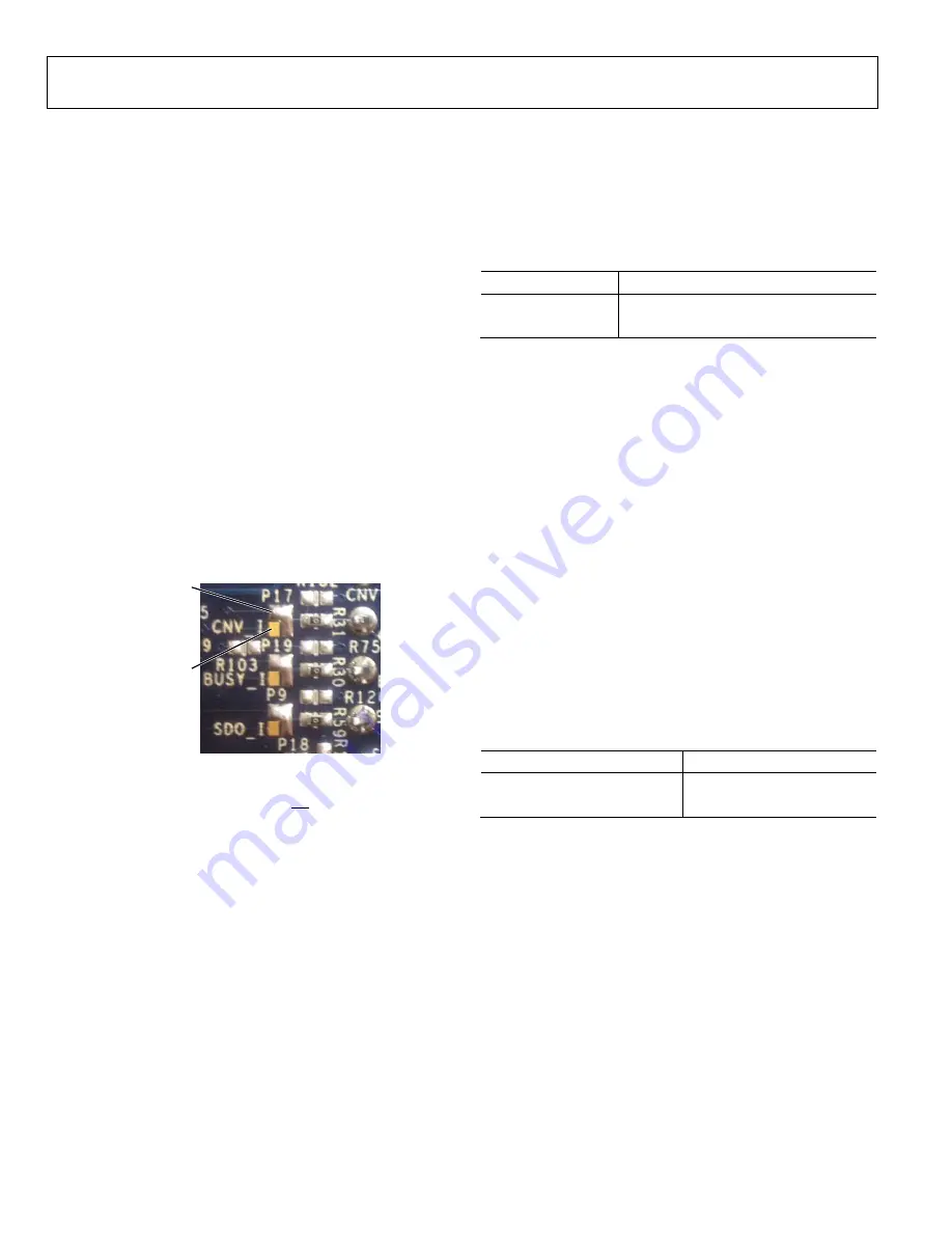
by modifying the default solder pad connections. As shown
in Figure 2, each digital signal on the
ADAS3022
is connected
to the larger (top) pad of the three. The default configuration
is the small pad and larger pad (no text) which connects the
FPGA to the
ADAS3022
(CNV, BUSY, and SDO signals
shown). The labeled pads, CNV_I, BUSY_I, SDO_I, and so
on, are the signals that are routed to P3. To use P3 instead of the
FPGA, unsolder the default connections and resolder from the
large pad to the xxx_I pads. The FPGA will remain powered;
however, if all the signals are bypassed in this fashion, it will
not have any influence on the
ADAS3022
.
Figure 2. Digital Interface Solder Pads—Partial View
Serial Interface
The 4-wire serial interface consisting of CS, DIN, SCK, and
SDO is present on the digital interface test points and is
controlled by the FPGA. The FPGA can be bypassed by using
the solder pads.
REFERENCE
The
ADAS3022
has an internal 4.096 V reference, along with an
internal buffer, useful for using an external reference or one can
use an external 4.096 V reference directly, such as the
ADR434
provided on the evaluation board. The evaluation board can be
configured to use any of these references. Two jumpers (P5
and P9) are used for setting the reference in conjunction with
software control.
External Reference–Factory Configuration
The evaluation board includes the
ADR434
, A1, which is a
4.096 V precision voltage reference. This reference can drive
the ADC REF1 or REF2 (REFx) pin directly or it can also be
buffered with U20, the
AD8032
; both of these are set to the
factory default setting.
Table 2. Factory Reference Jumper Configuration
Jumper
Setting
P5
REFIN to GND
1
P9
REF to BUF (U20)
1
The connection is made through R102 = 10 k to GND.
To use another reference source, there are two methods:
•
For an external unbuffered reference, remove the P9
jumper and connect a source to the REF test point.
•
Since the
ADR434
is a standard 8-lead SOIC, it can also
be removed and replaced with the user’s reference. In this
case, the user reference and the U20
AD8032
buffer can
be used as a reference source.
Internal 4.096 V Reference
The ADC has an internal 4.096 V precision reference and
can be used on most applications. When enabled, 4.096 V will
be present on the
ADAS3022
REFx pin and test point, REF. In
addition, a voltage will also be present on the
ADAS3022
REFIN pin and test point, REFIN. The voltage present on
REFIN can be used for other purposes, such as to provide the
bias voltage; however, it would need a suitable buffer as the
output impedance of the REFIN is on the order of a few kilo
ohms and loading this voltage down will degrade the internal
reference’s performance.
Table 3. Internal Reference Jumper Configuration
Jumper
Setting
P5
Open
P9
Open
Note that the
ADAS3022
configuration register needs to be
updated either using the included software or by writing the
appropriate bits to enable the internal reference.
Internal Reference Buffer
The internal reference buffer is useful when using an external
2.5 V reference. When using the internal reference buffer,
applying 2.5 V to REFIN, which is directly connected to the
ADC’s REFIN pin, produces 4.096 V at the ADCs REFx pin
and REF test point.
Note that the
ADAS3022
configuration register needs to be
updated either using the included software or by writing the
appropriate bits to enable the internal reference buffer.
DEFAULT
CONNECTION TO P3
1
1064-
003


