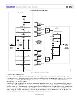


UG-1262
Rev. B | Page 80 of 312
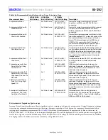
OFFSET CALIBRATION VOLTAGE INPUT CHANNEL (PGA GAIN = 2) REGISTER
Address: 0x400C22C8, Reset: 0x00000000, Name: ADCOFFSETGN2
Table 88. Bit Descriptions for ADCOFFSETGN2
Bits Bit
Name Settings
Description
Reset
Access
[31:15] Reserved
Reserved.
0x0 R
[14:0] VALUE
Offset Calibration Voltage Channel Gain 2. ADC offset correction for inputs using
PGA gain = 2, represented as a twos complement number. The calibration resolution
is 0.25 LSBs of the ADCDAT LSB size.
0x0 R/W
0x3FFF
4095.75 (maximum positive offset calibration value).
0x0001
0.25 (minimum positive offset calibration value).
0x0000
0 (no offset adjustment).
0x7FFF
−0.25 (minimum negative offset calibration value).
0x4000
−4096 (maximum negative offset calibration value).
GAIN CALIBRATION VOLTAGE INPUT CHANNEL (PGA GAIN = 2) REGISTER
Address: 0x400C2274, Reset: 0x00004000, Name: ADCGAINGN2
Table 89. Bit Descriptions for ADCGAINGN2
Bits Bit
Name
Settings
Description
Reset
Access
[31:15] Reserved
Reserved.
0x0
R
[14:0] VALUE
Gain Calibration PGA Gain 2. ADC gain correction for voltage input channels.
Stored as a signed number. Bit 14 is the sign bit and Bits[13:0] represent the
fractional part.
0x4000 R/W
0x7FFF
2 (maximum positive gain adjustment).
0x4001
1.000061 (minimum positive gain adjustment).
0x4000
1.0. ADC result multiplied by 1. No gain adjustment. Default value.
0x3FFF
0.999939 (minimum negative gain adjustment).
0x2000
0.5. ADC result multiplied by 0.5.
0x0001
0.000061 (maximum negative gain adjustment).
0x0000
0. Invalid value. Results in ADC result of 0.
OFFSET CALIBRATION VOLTAGE INPUT CHANNEL (PGA GAIN = 4) REGISTER
Address: 0x400C22D4, Reset: 0x00000000, Name: ADCOFFSETGN4
Table 90. Bit Descriptions for ADCOFFSETGN4
Bits Bit
Name Settings
Description
Reset
Access
[31:15] Reserved
Reserved.
0x0 R
[14:0]
VALUE
Offset Calibration Gain 4. ADC offset correction with PGA gain = 4.
0x0
R/W
0x3FFF
4095.75 (maximum positive offset calibration value).
0x0001
0.25 (minimum positive offset calibration value).
0x0000
0 (no offset adjustment).
0x7FFF
−0.25 (minimum negative offset calibration value).
0x4000
−4096 (maximum negative offset calibration value).