Parallel Port Interrupt
8-12
ADSP-2126x SHARC Processor Hardware Reference
twice as fast as the 8-bit port, as the overhead for
ALE
cycles is zero.
This is convenient when interfacing to high speed 16-bit
FIFO-based devices, including A/D and D/A converters.
• In situations where a majority of address accesses are non-sequen-
tial and cross 256 byte boundaries, the overhead of the
ALE
cycles
in the 8-bit mode approaches 20%
1
. In this particular situation,
the 16-bit memory can provide a 40% speed advantage over the
8-bit mode.
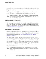
Parallel Port Interrupt
The parallel port has one interrupt signal,
PPI
, (bit 3 in the
LIRPTL
regis-
ter). When DMA is enabled, the maskable interrupt
PPI
occurs when the
DMA block transfer has completed (when the DMA Internal Word Count
register
ICPP
decrements to zero). When DMA is disabled, the maskable
interrupt is latched in every cycle the receive buffer is not empty or the
transmit buffer is not full.
The parallel port receive (
RXPP
) and transmit (
TXPP
) buffers are memory
mapped IOP registers. The
PPI
bit is located at vector address 0x50. The
latch (
PPI
), mask (
PPIMSK
) and mask pointer (
PPIMSKP
) bits associated
with the parallel port interrupt are all located in the
LIRPTL
register.
Parallel Port Throughput
As described in
, each 32-bit word transferred
through the parallel port takes a specific period of time to complete. This
throughput depends on a number of factors, namely parallel port speed
(1/3 core instruction rate), memory width (8 bits or 16 bits), and memory
1
This can be realized by recalling that four bytes must be packed/unpacked into a single 32-bit word.
For example when a 32-bit word is written/read, there is a single ALE cycle inserted per four consecu-
tive addresses. This results in: (N/4 ALE cycles)/(N ac N/4 ALE cycles) x 100% = 20%.
Summary of Contents for ADSP-21261 SHARC
Page 30: ...Contents xxx ADSP 2126x SHARC Processor Hardware Reference ...
Page 40: ...Register Diagram Conventions xl ADSP 2126x SHARC Processor Hardware Reference ...
Page 58: ...Differences From Previous SHARCs 1 18 ADSP 2126x SHARC Processor Hardware Reference ...
Page 112: ...Secondary Processing Element PEy 2 54 ADSP 2126x SHARC Processor Hardware Reference ...
Page 178: ...Summary 3 66 ADSP 2126x SHARC Processor Hardware Reference ...
Page 204: ...DAG Instruction Summary 4 26 ADSP 2126x SHARC Processor Hardware Reference ...
Page 322: ...Setting Up DMA 7 32 ADSP 2126x SHARC Processor Hardware Reference ...
Page 436: ...SPORT Programming Examples 9 86 ADSP 2126x SHARC Processor Hardware Reference ...
Page 521: ...ADSP 2126x SHARC Processor Hardware Reference 11 31 Input Data Port rts IDP_ISR end ...
Page 522: ...Input Data Port Programming Example 11 32 ADSP 2126x SHARC Processor Hardware Reference ...
Page 590: ...Timer Programming Examples 14 20 ADSP 2126x SHARC Processor Hardware Reference ...
Page 796: ...I O Processor Registers A 174 ADSP 2126x SHARC Processor Hardware Reference ...
Page 800: ...B 4 ADSP 2126x SHARC Processor Core Manual ...
Page 846: ...Index I 36 ADSP 2126x SHARC Processor Hardware Reference ...


