background image


AD9959/PCB


Rev. 0 | Page 5 of 28 

EVALUATION BOARD SOFTWARE

INSTALLING THE SOFTWARE 

Follow these steps to install the AD9959 evaluation software: 

1.


Log into your PC system with administrative privileges; 
this is an essential requirement in successfully installing 
the AD9959 evaluation software. 

2.


Uninstall any previous versions of the AD9959 evaluation 
software from your PC system. 

3.


Insert the AD9959 evaluation software CD into your  
CD-ROM drive. It is important not to connect the  
AD9959 evaluation board to the computer until the 
AD9959 evaluation software has been successfully 
installed. Refer to the 

Readme.txt

 file located in the 

Software

 folder before proceeding with the installation  

of the AD9959 evaluation software.  

4.


Run the 

setup.exe

 file located in the 

Software

 folder and 

follow the AD9959 evaluation software’s on-screen 
installation instructions. 

CONFIGURING THE EVALUATION BOARD 

Once the software has been successfully installed onto your PC, 
the next step is to interface the AD9959 evaluation software to 
the AD9959 evaluation board via the USB Port (see Figure 2). 

In order for the evaluation board and software to communicate 
properly, drivers must be loaded onto your PC system. The 
following instructions explain how to install these drivers on 
your PC system.  

Windows 98/ME/2000 Users 

1.


Power up the AD9959 evaluation board (see Table 2). 

2.


Connect the evaluation board to the computer using a USB 
cable via the USB port; the VBUS LED (CR1 on AD9959 
evaluation board) illuminates. 

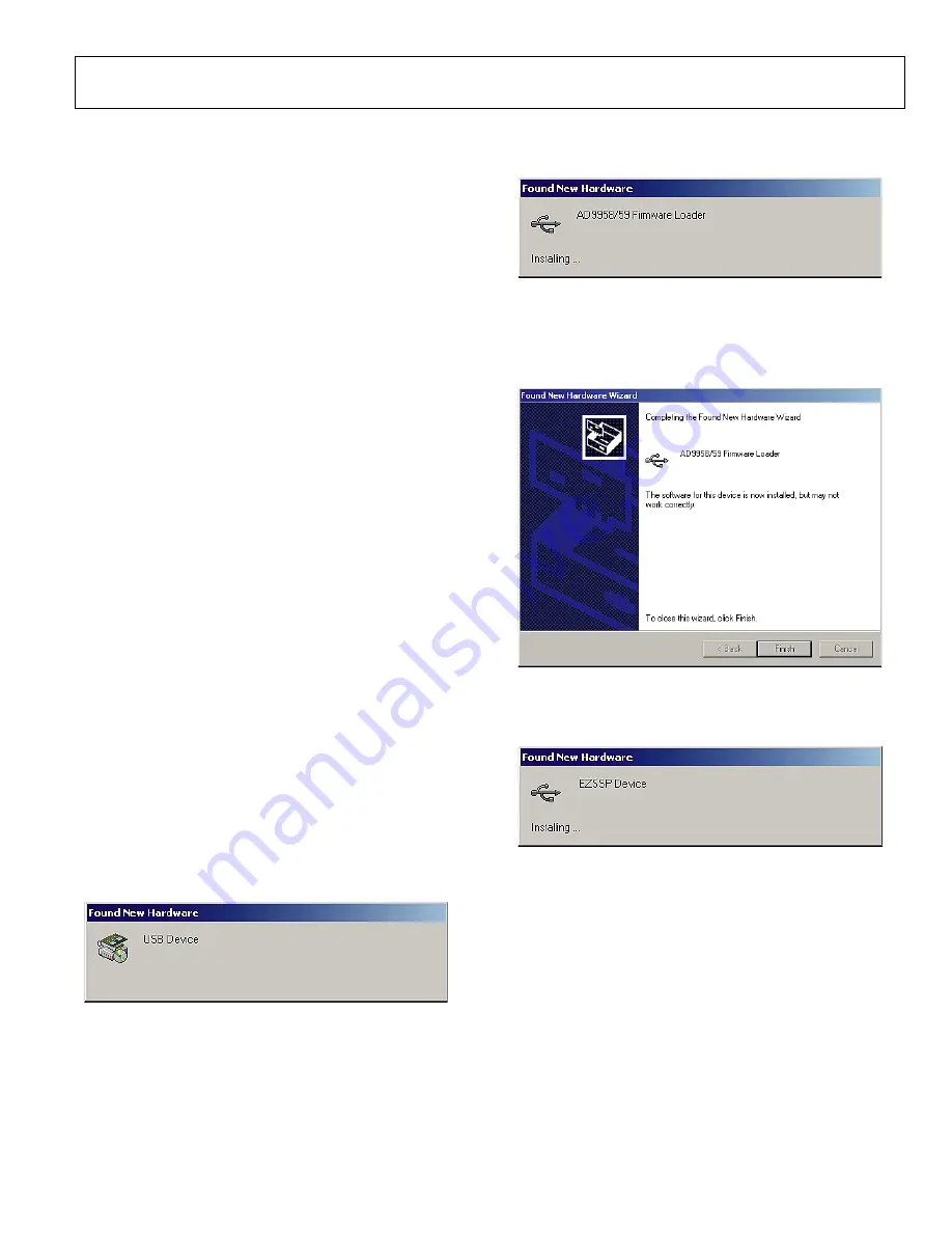
3.


When the USB cable is connected, this window appears 
and then disappears (Figure 3). 

05698-

003


Figure 3. 


4.


Then, this window (Figure 4) also appears and disappears. 

05698-

004


Figure 4.  


5.


If you are using Windows 2000, click 

Finish

 if you see this 

window (Figure 5). 


05698-

005


Figure 5.  

 
6.


Next, the window in Figure 6 appears. 


05698-

006


Figure 6.  

After the window has disappeared, the USB Status LED (CR2 
on AD9959 evaluation board) flashes, which indicates that the 
evaluation board is connected properly. 

Summary of Contents for AD9959/PCB

Page 1: ...nderutilized and idle equipment along with credit for buybacks and trade ins Custom engineering so your equipment works exactly as you specify Critical and expedited services Leasing Rentals Demos In...

Page 2: ...CLK J9 REFCLK MULTIPLIER 4 TO 20 J13 J11 J12 SYNC CLK SYNC IN SYNC OUT 4 SYS CLK TIMING AND CONTROL LOGIC DDS 1 AD9959 EVALUATION BOARD Figure 1 FEATURES Full featured evaluation board for the AD9959...

Page 3: ...valuation Board Software 5 Installing the Software 5 Configuring the Evaluation Board 5 Windows 98 ME 2000 Users 5 Windows XP Users 6 Loading the Software 7 Status Messages upon Loading Software 8 Fea...

Page 4: ...VCC_USB 3 3 TB1 2 DVDD_I O 3 3 TB1 3 GND 0 TB1 4 DVDD 1 8 J10 CLK_VDD 1 8 J16 AVDD 1 8 J17 AVDD 1 8 J18 BG_VDD 1 8 J19 AVDD 1 8 J20 AVDD 1 8 Note that the AD9959 PCB is preconfigured so that the CLK_...

Page 5: ...59 s clock input circuitry Clock Mode Select Controls whether the part is driven by a 20 MHz to 30 MHz crystal provided by the user or by an external signal generator such as Ref Clk Ref Clk Input Inp...

Page 6: ...OARD Once the software has been successfully installed onto your PC the next step is to interface the AD9959 evaluation software to the AD9959 evaluation board via the USB Port see Figure 2 In order f...

Page 7: ...rd illuminates 3 When the USB cable is connected the screen below appears Figure 7 Click Next to continue 05698 007 Figure 7 4 Click Continue Anyway when you see the window in Figure 8 05698 008 Figur...

Page 8: ...are make sure that the AD9959 evaluation board is powered up connected to the computer and that the USB Status LED is flashing 2 Click on the Start button located at the bottom left hand corner of you...

Page 9: ...15 Scrolling up through the status box with the cursor will indicate why the software did not load correctly Most status message errors can be resolved by checking jumper settings making sure that the...

Page 10: ...AD9959 evaluation software is set to Auto I O Update so that when LOAD is clicked an I O update signal is automatically sent to the device If synchronization across channels is desired use the Manual...

Page 11: ...file Pin 3 to control this feature using only Profile Pin 3 If you wish to use the SDIO data pins to control this feature simply select Use SDIO pins 1 2 3 Note that to use the SDIO pins to control th...

Page 12: ...section in the Level box 4 Linear Sweep Options Use the Linear Sweep Options section to control the linear sweep features Select Enable Linear Sweep to turn on the linear sweep function and the addit...

Page 13: ...ct either Full Scale default setting Scale Scale or Scale for the DAC output current See the Scalable DAC Reference Current Control Mode section of the AD9959 data sheet 7 Output Waveform In the Outpu...

Page 14: ...the linear frequency sweep and the first level in frequency modulation FSK Phase Offset consists of two boxes In the first box set the integer factor 1 999 to increment or decrement the phase offset...

Page 15: ...to the device 2 Profile Registers The AD9959 features up to 16 programmable registers per channel as shown in Figure 23 Due to certain channel constraints however there are limitations on how the Prof...

Page 16: ...ection of the AD9959 data sheet 4 Linear Sweep Setup Use the Linear Sweep Setup section to setup the slope of the linear sweep In the Rising Step Size box enter the desired value for the rising step s...

Page 17: ...erial port state machine Select LSB First to change the data format to LSB first from the default setting of MSB first Use the Serial I O Mode drop menu to select the desired serial I O mode of operat...

Page 18: ...les serve as a reference and or starting point when trying to configure the device for a desired setup for the first time To load these setup files click File and select Load Setup Figure 33 or click...

Page 19: ...The Chip Level Control window Figure 37 from this particular setup shows that a 500 MHz System Clock is running with the RU RD operation enabled In the RU RD box Use Profile Pins 2 3 has been selecte...

Page 20: ...ction P0 controls Channel 0 P1 controls Channel 1 P2 controls Channel 2 and P3 controls Channel 3 If a profile pin is deselected the associated channel s output will return to 0 MHz To return to full...

Page 21: ...010 Referring to the table in the 16 Level Modulation No RU RD section of the AD9959 data sheet we see that this bit pattern sets up 16 level modulation on Channel 2 05698 041 Figure 41 In the Channel...

Page 22: ...output frequency is equivalent to the value entered in the Frequency 00 box 3 MHz in this setup If all profile pins are pressed the output frequency is equal to 48 MHz the contents of Profile Registe...

Page 23: ...to ensure synchronization across channels and reinitialize the starting point once the linear sweep ends 05698 045 Figure 45 In the Channel Control window Figure 46 each channel has Amplitude selecte...

Page 24: ...ing that the sweep begins at half scale and sweeps up to full scale Amplitude 01 ending point of sweep In the Linear Sweep Setup section the rising falling step size and step intervals of the sweep ar...

Page 25: ...2 1 4 5 6 R6 50 R5 50 ADTT1 1 AVDD1 AVDD1 AVDD3 DAC3_OUT GND 3 2 1 4 5 6 R8 50 R7 50 ADTT1 1 AVDD0 AVDD0 T4 T5 DAC1 AD9958 DAC3 AD9959 DAC0 AD9958 DAC2 AD9959 GND R11 1 91k ETC1 1 13 1 5 3 4 T1 PRI SE...

Page 26: ...L9 DAC 1 DUT FILTER OUT J5 DAC 1 AD9959 DUT OUT FILTER IN R22 0 R23 0 DAC1_OUT J1 200MHz LOW PASS FILTER C72 _F C76 _F C71 _F C74 _F C73 _F C75 _F C80 _F C77 _F C78 _F L5 GND GND GND GND GND GND GND G...

Page 27: ...7 18 19 20 21 22 23 24 25 26 27 28 PD4 FD12 PD3 FD11 PD2 FD10 PD1 FD9 PD0 FD8 WAKEUP VCC7 RESET GND6 PA7 FLAGD SLC5 PA6 PKTEND PA5 FIFOADR1 PA4 FIFOADR0 PA3 WU2 PA2 SLOE PA1 INT1 PA0 INT0 VCC6 CTL2 FL...

Page 28: ...charges as high as 4000 V readily accumulate on the human body and test equipment and can discharge without detection Although this product features proprietary ESD protection circuitry permanent dam...

Page 29: ...AD9959 PCB Rev 0 Page 28 of 28 2005 Analog Devices Inc All rights reserved Trademarks and registered trademarks are the property of their respective owners EB05698 0 10 05 0 NOTES...

Page 30: ...uipment Have surplus equipment taking up shelf space We ll give it a new home Learn more Visit us at artisantg com for more info on price quotes drivers technical specifications manuals and documentat...

Reviews: