


AD5934
Rev. A | Page 16 of 40
2-POINT CALIBRATION
Alternatively, it is possible to minimize this error by assuming
that the frequency variation is linear and adjusting the gain
factor with a 2-point calibration. Figure 19 shows an impedance
profile based on a 2-point gain factor calculation.
101.5
98.5
54
66
0
532
5-
0
86
FREQUENCY (kHz)
IM
P
E
D
ANCE
(
k
Ω
)
101.0
100.5
100.0
99.5
99.0
56
58
60
62
64
VDD = 3.3V
CALIBRATION FREQUENCY = 60kHz
T
A
= 25°C
MEASURED CALIBRATION IMPEDANCE = 100k
Ω
Figure 19. Impedance Profile Using a 2-Point Gain Factor Calculation
2-POINT GAIN FACTOR CALCULATION
This is an example of a 2-point gain factor calculation assuming
the following:
Output excitation voltage = 2 V p-p
Calibration impedance value, Z
UNKNOWN
= 100.0 kΩ
PGA gain = ×1
Supply voltage = 3.3 V
Current-to-voltage amplifier gain resistor = 100 kΩ
Calibration frequencies = 55 kHz and 65 kHz
Typical values of the gain factor calculated at the two calibration
frequencies read
Gain factor calculated at 55 kHz is 1.031224 × 10
−9
.
Gain factor calculated at 65 kHz is 1.035682 × 10
−9
.
Difference in gain factor (ΔGF) is
1.035682 × 10
−9
− 1.031224 × 10
−9
= 4.458000 × 10
−12
.
Frequency span of sweep (ΔF) is 10 kHz.
Therefore, the gain factor required at 60 kHz is given by
9
-
10
1.031224
kHz
5
kHz
10
12
-
4.458000E
×
+
⎟
⎠
⎞
⎜
⎝
⎛
×
The required gain factor is 1.033453 × 10
−9
.
The impedance is calculated as previously described in the
Impedance Calculation section.
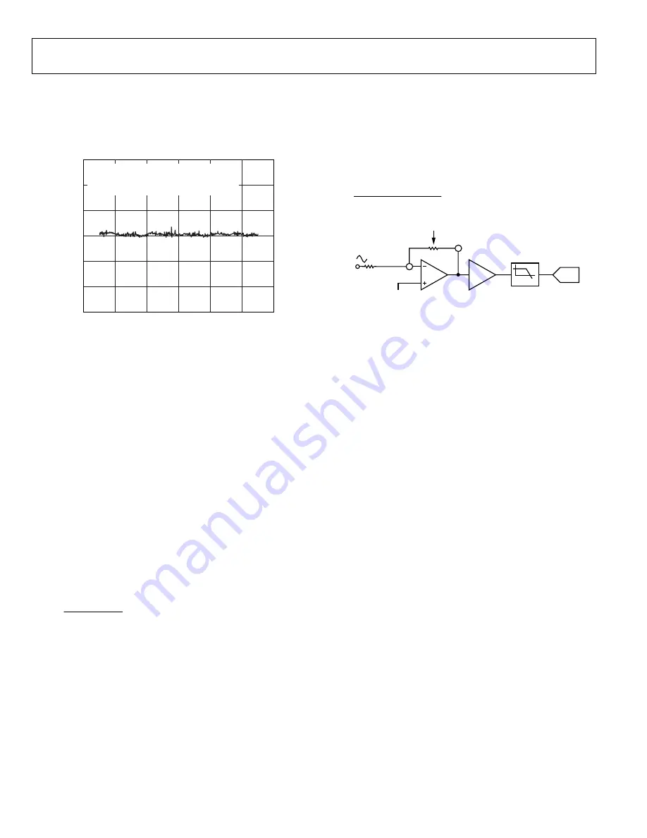
GAIN FACTOR SETUP CONFIGURATION
When calculating the gain factor, it is important that the receive
stage is operating in its linear region. This requires careful selection
of the excitation signal range, current-to-voltage gain resistor
and PGA gain. The gain through the system shown in Figure 20
is given by
Output Excitation Voltage Range
×
UNKNOWN
Z
Resistor
Setting
Gain
×
PGA Gain
05
32
5-
0
89
VIN
VDD/2
RFB
ADC
LPF
Z
UNKNOWN
VOUT
CURRENT-TO-VOLTAGE
GAIN SETTING RESISTOR
PGA
(×1 OR ×5)
Figure 20. System Voltage Gain
For this example, assume the following system settings:
VDD = 3.3 V
Gain setting resistor = 200 kΩ
Z
UNKNOWN
= 200 kΩ
PGA setting = ×1
The peak-to-peak voltage presented to the ADC input is 2 V p-p.
However, had the user chosen a PGA gain of ×5, the voltage
would saturate the ADC.
GAIN FACTOR RECALCULATION
The gain factor must be recalculated for a change in any of the
following parameters:
•
Current-to-voltage gain setting resistor
•
Output excitation voltage
•
PGA gain
Summary of Contents for AD5934
Page 35: ...AD5934 Rev A Page 35 of 40 SCHEMATICS 05325 144 Figure 40 EVAL AD5934EBZ USB Schematic ...
Page 36: ...AD5934 Rev A Page 36 of 40 05325 145 Figure 41 EVAL AD5934EBZ Schematic ...
Page 37: ...AD5934 Rev A Page 37 of 40 05325 146 Figure 42 Linear Regulator on EVAL AD5934EBZ ...
Page 38: ...AD5934 Rev A Page 38 of 40 05325 147 Figure 43 Decoupling on the EVAL AD5934EBZ ...