B14 PWR
+3.3VCable
power
B15 PWR
+3.3VCable
power
B16
PWR RTN
Cable power return
B17
PWR RTN
Cable power return
B18 CWAKEn
Power management signal for
wakeup events (optional)
B19 CPERSTn
Cable
PERSTn
13
3.3
3.3
Switches
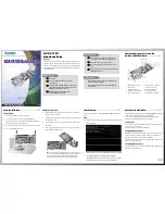
Switches
The PCA contains x2 and x8 switches that allow configuration of the PCA PCIe mode (SW1),
equalization and de-emphasis (SW2). The two switches, SW1 and SW2, are located on top of the
front side of the PCA card.
Figure 3-5
show the location of the board.
Figure 3-5 Switches