background image

Chapter 2:  Board Components

2–21

Components and Transceiver Interfaces

© March 2010  Altera Corporation

Cyclone IV GX Transceiver Starter Board Reference Manual

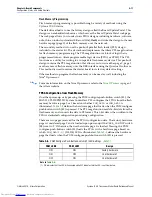
10/100/1000 Ethernet

A Marvell 88E1111 PHY device is used for 10/100/1000 BASE-T Ethernet connection. 
The device is an auto-negotiating Ethernet PHY with an SGMII interface to the FPGA. 
The MAC function must be provided in the FPGA for typical networking applications 
such the Altera Triple Speed Ethernet MegaCore design. The Marvell 88E1111 PHY 
uses 2.5-V and 1.2-V power rails and requires a 25-MHz reference clock driven from a 
dedicated oscillator. The device interfaces to a Halo Electronics HFJ11-1G02E model 
RJ45 with internal magnetics that can be used for driving copper lines with Ethernet 
traffic.

By default, the 

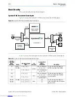
GXB_RX1

 and 

GXB_TX1

 channels of the FPGA are connected to the 

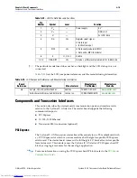
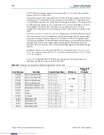
Ethernet PHY as shown in 

Table 2–27 on page 2–22

.

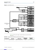
Figure 2–6

 shows the SGMII interface between the FPGA (MAC) and Marvell 88E1111 

PHY.

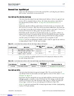
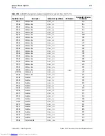
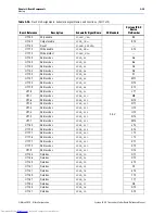
Table 2–25

 lists the Ethernet PHY interface pin assignments.

Table 2–26

 lists the Ethernet PHY interface component reference and manufacturing 

information.

Figure 2–6. 

SGMII Interface between FPGA (MAC) and Marvell 88E1111 PHY

10/100/1000 Mbps

Ethernet MAC

Marvell 88E1111

PHY

Device

RJ45

SGMII Interface

Table 2–25. 

Ethernet PHY Pin Assignments, Signal Names and Functions

Board Reference

Description

Schematic Signal Name

I/O Standard

Cyclone IV GX 

Device 

Pin Number

U9.82

SGMII TX data

ENET_TX_P

1.4-V PCML

C2

U9.81

SGMII TX data

ENET_TX_N

C1

U9.77

SGMII RX data

ENET_RX_P

E2

U9.75

SGMII RX data

ENET_RX_N

E1

U9.25

Management bus control

ENET_MDC

2.5-V

N9

U9.24

Management bus data

ENET_MDIO

K8

U9.23

Management bus interrupt

ENET_INTn

F12

U9.28

Device reset

ENET_RESETn

K9

Table 2–26. 

Ethernet PHY Component Reference and Manufacturing Information

Board 

Reference

Description

Manufacturer

Manufacturing

Part Number

Manufacturer 

Website

U9

Ethernet PHY BASE-T device

Marvell Semiconductor

88E1111-B2-CAAIC000

www.marvell.com

Downloaded from 

Elcodis.com


electronic components distributor


Summary of Contents for Cyclone IV GX

Page 1: ...vation Drive San Jose CA 95134 www altera com Cyclone IV GX Transceiver Starter Board Reference Manual Document Version 1 0 Document Date March 2010 Downloaded from Elcodis com electronic components distributor ...

Page 2: ...ations maskwork rights and copyrights Altera warrants performance of its semiconductor products to current specifications in accordance with Altera s standard warranty but reserves the right to make changes to any products and services at any time without notice Altera assumes no responsibility or liability arising out of the application or use of any information product or service described herei...

Page 3: ...2 12 FPGA Configuration using EPCS Device 2 12 Status Elements 2 13 Setup Elements 2 13 Board Settings DIP Switch 2 14 Configuration Settings DIP Switch 2 14 Configuration Push Button Switches 2 15 Clock Circuitry 2 16 Cyclone IV GX Transceiver Clock Inputs 2 16 General User Input Output 2 17 User Defined Push Button Switches 2 17 User Defined LEDs 2 17 LCD 2 18 Components and Transceiver Interfac...

Page 4: ...iv Cyclone IV GX Transceiver Starter Board Reference Manual March 2010 Altera Corporation ary Downloaded from Elcodis com electronic components distributor ...

Page 5: ...m for developing and prototyping low power high volume feature rich designs as well as to demonstrate the Cyclone IV GX device s on chip memory embedded multipliers and the Nios II embedded soft processor The board provides peripherals and memory interfaces to facilitate the development of the Cyclone IV GX transceiver designs The Cyclone IV GX transceiver starter board is especially suitable for ...

Page 6: ...rcuitry MAX II CPLD EPM2210 System Controller and flash passive serial PS configuration On board USB BlasterTM for use with the Quartus II Programmer JTAG header for external USB Blaster with the Quartus II Programmer Erasable programmable configurable serial EPCS device On Board ports USB 2 0 One gigabit Ethernet port Transceiver interfaces PCI Express x1 edge connector 10 100 1000BASE T Ethernet...

Page 7: ...button switch One MAX II configuration reset push button switch One PGM configure push button switch configure the FPGA from flash memory One PGM select push button switch select image to load from flash memory Two general user push button switches DIP switches Board setting DIP switch Configuration setting DIP switch Power supply 9 V 16 V DC input 2 5 mm barrel jack for DC power input On Off slid...

Page 8: ...c Without proper anti static handling the board can be damaged Therefore use anti static handling precautions when touching the board Figure 1 1 Cyclone IV GX transceiver Starter Board Block Diagram 2x16 LCD User LEDs CPLD EPM2210 System Controller 128 Mb Flash 18 Mb SSRAM Gigabit Ethernet PHY SGMII Clock_SMA Embedded USB Blaster USB 2 0 x4 x4 x3 JTAG Chain SMA EPCS x4 EP4CGX15BF14 x1 Edge 1st Cha...

Page 9: ...ration software refer to the Cyclone IV GX Transceiver Starter Kit User Guide This chapter consists of the following sections Board Overview Featured Device Cyclone IV GX Device on page 2 4 MAX II CPLD EPM2210 System Controller on page 2 6 Configuration Status and Setup Elements on page 2 9 Clock Circuitry on page 2 16 General User Input Output on page 2 17 Components and Transceiver Interfaces on...

Page 10: ...5 S6 MAX II CPLD EPM240 Embedded USB Blaster U4 Resistor Multiplexer R52 R53 Capacitor Multiplexer C58 C59 Table 2 1 Cyclone IV GX Transceiver Starter Board Components Part 1 of 3 Board Reference Type Description Featured Devices U8 FPGA EP4CGX15BF14 169 pin FBGA U10 CPLD EPM2210F256 256 pin FBGA Configuration Status and Setup Elements J5 USB Type B connector Connects to the computer to enable emb...

Page 11: ...0 MHz oscillator 50 MHz crystal oscillator for configuration purpose This oscillator is located at the bottom of the board J2 J3 Clock input SMAs Drive LVPECL compatible clock inputs into the clock multiplexer buffer U6 General User Input Output D5 D6 D7 D8 User LEDs Four user LEDs Illuminates when driven low S5 S6 User push button switches Two user push button switches Driven low when pressed J6 ...

Page 12: ... multiplexer Capacitor multiplexer which requires a minor modification on the board if the optional transceiver RX SMA connectors J8 J9 are used R51 R52 R53 R54 Transceiver TX resistor multiplexer Resistor multiplexer which requires a minor modification on the board if the optional transceiver TX SMA connectors J11 J10 are used Power Supply J4 DC input jack Accepts a 9 V 16 V DC power supply Do no...

Page 13: ...2 Bank Name Number of Channels Bank Name Number of I Os 2 GXB0 Table 2 4 Cyclone IV GX Device I O Pin Count and Usage Note 1 Function I O Standard I O Count Special Pins Flash SSRAM FSML Bus 2 5 V CMOS 47 1 DEV_OE Gigabit Ethernet 4 Buttons 3 1 DEV_CLRn LCD 1 LEDs 4 1 INIT_DONE 1 nCEO Clocks or Oscillators 2 5 V CMOS LVDS 7 3 differential clock input pair 1 clock input PCI Express 2 5 V CMOS 1 Pas...

Page 14: ... relative to the MAX II device U10 Figure 2 3 MAX II CPLD EPM2210 System Controller Block Diagram Information Register MAX II Embedded USB Blaster MAX II CPLD EPM2210 System Controller Power Calculations SLD HUB PFL Power Measurement Results Virtual JTAG PC EP4CGX15 LTC2418 Controller FLASH Decoder Encoder JTAG Control SSRAM Control Register LCD GPIO Table 2 5 MAX II CPLD EPM2210 System Controller...

Page 15: ...C6 FSML bus address FSML_A4 M15 A8 FSML bus address FSML_A5 M16 A7 FSML bus address FSML_A6 L15 M11 FSML bus address FSML_A7 L16 N12 FSML bus address FSML_A8 K15 K10 FSML bus address FSML_A9 K16 L11 FSML bus address FSML_A10 J15 M9 FSML bus address FSML_A11 J16 N10 FSML bus address FSML_A12 H16 N11 FSML bus address FSML_A13 H15 H10 FSML bus address FSML_A14 G16 H12 FSML bus address FSML_A15 G15 N1...

Page 16: ...tch MAX_CSn T12 L5 MAX II chip select PGM_CONFIG R10 Loads flash memory image identified by the PGM LEDs PGM_LED0 T9 Flash memory PGM select indicator 0 PGM_LED1 R9 Flash memory PGM select indicator 1 PGM_SEL T10 Toggles the PGM_LED 0 1 sequence SENSE_CSn J3 Power monitor chip select SENSE_SCK J1 Power monitor serial peripheral interface SPI clock SENSE_SDI J2 Power monitor SPI data in SENSE_SDO K...

Page 17: ...he FPGA using an external USB Blaster Serial configuration EPCS device U15 is used to store configuration data for FPGA device that supports active serial AS configuration and reloads the data to the FPGA upon power up or reconfiguration FPGA Configuration over Embedded USB Blaster The USB Blaster is implemented using a USB Type B connector J5 a FTDI USB 2 0 PHY device U5 and an Altera MAX II CPLD...

Page 18: ...ine and control logic to determine the configuration source for the Cyclone IV GX FPGA Table 2 7 lists the Cyclone IV GX configuration modes Figure 2 4 JTAG Chain GPIO TCK EP4CGX15BF14 FPGA MAX II CPLD EPM2210 System Controller GPIO TMS GPIO TDO GPIO TDI USB_DISABLE TCK TMS TDI TDO JTAG 2 x 5 Header Flash 128 Mb USB PHY PCI Express Edge Gold Finger TCK TMS TDI TDO TCK TMS TDI TDO MAX II EPM240M100...

Page 19: ...he flash memory can be used as well including the Nios II processor f For more information on the Nios II processor refer to the Nios II Processor page of the Altera website FPGA Configuration from Flash Memory On either power up or by pressing the PGM configure push button switch S1 the MAX II CPLD EPM2210 System Controller s PFL configures the FPGA from the flash memory hardware page 0 or 1 base...

Page 20: ...PCS device set the configuration DIP switch S7 to select the AS configuration scheme as shown in Table 2 13 on page 2 14 After programming the EPCS device the design is loaded from the EPCS device to the FPGA when you power up the board EPCS Programming EPCS programming is possible through a variety of methods One method to program the EPCS device is to use the Serial FlashLoader SFL a JTAG based ...

Page 21: ...when PGM select push button switch is pressed Driven by the MAX II CPLD EPM2210 System Controller D12 Power Blue LED Illuminates when 9 V 16 V power is active D13 USB_LED Green LED Illuminates when the embedded USB Blaster is in use to program the FPGA Driven by the MAX II CPLD EPM2210 System Controller and MAX IIZ D14 ENET_LEDR_TX Green LED Illuminates to indicate Ethernet PHY transmit activity D...

Page 22: ...2 USER_PGM ON Load user hardware page 1 from flash memory upon power up OFF Load factory design from flash memory upon power up OFF S8 3 EPM2210_JTAG_EN ON Bypass Max II CPLD EPM2210 System Controller OFF Max II CPLD EPM2210 System Controller in chain OFF S8 4 PCIE_JTAG_EN ON Bypass PCI Express OFF PCI Express in chain ON Note to Table 2 11 1 ON indicates a setting of 0 while OFF indicates a setti...

Page 23: ...ation push button switches component reference and manufacturing information JTAG JTAG based configuration X 2 Notes to Table 2 13 1 ON indicates a setting of 0 while OFF indicates a setting of 1 2 X indicates does not care The JTAG based configuration takes precedence over other configuration schemes and therefore the FPGA_MSEL pin settings are ignored Table 2 13 Configuration Settings DIP Switch...

Page 24: ... LVDS LVDS LVDS CMOS CMOS Edge Gold Finger Table 2 16 Cyclone IV GX Transceiver Starter Board Clock Inputs Source Component Board Reference Source Schematic Signal Name I O Standard Cyclone IV GX Device Pin Number Description J3 SMA or 125 MHz CLKIN_SMA_P LVPECL M7 or E7 depending on CLK_SEL Positive and negative differential LVPECL clock inputs from SMAs J2 CLKIN_SMA_N N7 or E6 depending on CLK_S...

Page 25: ... names and their corresponding Cyclone IV GX device pin numbers Table 2 18 lists the user defined push button switch component reference and the manufacturing information User Defined LEDs The starter board includes four general purpose LEDs This section describes all user defined LEDs For information on board specific or status LEDs refer to Status Elements on page 2 13 Board references D5 throug...

Page 26: ...ned LED Schematic Signal Names and Functions Board Reference Description Schematic Signal Name I O Standard Cyclone IV GX Device Pin Number D8 User defined LEDs Driving a logic 0 on the I O port turns the LED ON Driving a logic 1 on the I O port turns the LED OFF USER_LED0 2 5 V N8 D7 USER_LED1 C13 D6 USER_LED2 N5 D5 USER_LED3 M6 Table 2 20 User Defined LED Component Reference and Manufacturing In...

Page 27: ...ard comes with a full height I O bracket for its low profile form factor card This interface uses the Cyclone IV GX device s PCI Express hard IP block saving logic resources for the user logic application f For more information on using the PCI Express hard IP block refer to the PCI Express Compiler User Guide Table 2 22 LCD Pin Definitions and Functions Pin Number Symbol Level Function 1 VDD Powe...

Page 28: ...termination is required This clock can have spread spectrum properties that change its period between 9 847 ps to 10 203 ps The I O standard is High Speed Current Steering Logic HCSL By default the GXB_RX0 channel of the FPGA is connected to the PCIE_RX_P and PCIE_RX_N signals while the GXB_TX0 channel is connected to the PCIE_TX_P and PCIE_TX_N signals Table 2 24 summarizes the PCI Express pin as...

Page 29: ...between the FPGA MAC and Marvell 88E1111 PHY Table 2 25 lists the Ethernet PHY interface pin assignments Table 2 26 lists the Ethernet PHY interface component reference and manufacturing information Figure 2 6 SGMII Interface between FPGA MAC and Marvell 88E1111 PHY 10 100 1000 Mbps Ethernet MAC Marvell 88E1111 PHY Device RJ45 SGMII Interface Table 2 25 Ethernet PHY Pin Assignments Signal Names an...

Page 30: ...apacitors and the multiplexer resistors are 0 Ω resistors Memory This section describes the board s memory interface support and also their signal names types and connectivity relative to the Cyclone IV GX device The board has the following memory interfaces SSRAM Flash SSRAM The SSRAM device consists of a single standard synchronous SRAM providing 18 Mb of memory with a 16 bit data bus This devic...

Page 31: ...dress bus FSML_A12 N11 U12 48 Address bus FSML_A13 H10 U12 49 Address bus FSML_A14 H12 U12 50 Address bus FSML_A15 N13 U12 80 Address bus FSML_A16 M13 U12 81 Address bus FSML_A17 J13 U12 82 Address bus FSML_A18 K13 U12 99 Address bus FSML_A19 L12 U12 100 Address bus FSML_A20 L13 U12 39 Address bus FSML_A21 K11 U12 58 Data bus FSML_D0 D11 U12 59 Data bus FSML_D1 D12 U12 62 Data bus FSML_D2 E10 U12 ...

Page 32: ...irection U12 85 Address status controller SRAM_ADSCn 2 5 V U12 84 Address status processor SRAM_ADSPn U12 83 Burst address advance SRAM_ADVn U12 93 Byte lane a write enable SRAM_BWan L4 U12 94 Byte lane b write enable SRAM_BWbn M4 U12 98 Chip enable SRAM_CEn N6 U12 89 Clock SRAM_CLK L7 U12 97 Chip enable SRAM_CE2 U12 92 Chip enable SRAM_CE3n U12 88 Global write enable SRAM_GWn U12 31 Burst sequenc...

Page 33: ...ess bus FSML_A7 N12 U11 19 Address bus FSML_A8 K10 U11 8 Address bus FSML_A9 L11 U11 7 Address bus FSML_A10 M9 U11 6 Address bus FSML_A11 N10 U11 5 Address bus FSML_A12 N11 U11 4 Address bus FSML_A13 H10 U11 3 Address bus FSML_A14 H12 U11 2 Address bus FSML_A15 N13 U11 1 Address bus FSML_A16 M13 U11 55 Address bus FSML_A17 J13 U11 18 Address bus FSML_A18 K13 U11 17 Address bus FSML_A19 L12 U11 16 ...

Page 34: ...ersus time Power Distribution System Figure 2 7 shows the power distribution system on the starter board The currents shown are conservative absolute maximum levels and reflects the regulator inefficiencies and sharing U11 40 Data bus FSML_D10 2 5 V A11 U11 42 Data bus FSML_D11 B11 U11 48 Data bus FSML_D12 B10 U11 50 Data bus FSML_D13 C11 U11 52 Data bus FSML_D14 C12 U11 54 Data bus FSML_D15 C8 Ta...

Page 35: ...CGX15 Core Voltage 1 2 V 1 083 A 1 2 V 1 634A 5 35V_MONITOR LT2418 5 35 V 0 010 A 2 5_VCC_GXB EP4CGX15 VCCH_GXB VCCA_GXB 2 5_VCCIO EP4CGX15 VCCIO Banks 2 5 V 0 057 A 2 5 V 0 025 A 9 V 16 V DC INPUT 6 345 W 9 V 0 705 A ideal diode mux 12 V PCI Express Motherboard 5 5 A Maximum 1 2_VCCD_PLL EP4CGX15 Digital PLL 1 2 V 0 07 A 5 0V Char LCD Linear Reg Input 3 3 V 0 02 A 3 3V Flash VCCD 5 0 V 0 005 A LT...

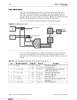
Page 36: ... the rail If no subnet is named the power is the total output power for that voltage Figure 2 8 Power Measurement Circuit SCK DSI DSO CSn 8 Ch Power Supply Load N Supply N RSENSE MAX II CPLD EPM2210 System Controller MAX II CPLD EPM240M100 USB PHY To User PC Power GUI JTAG Chain Embedded USB Blaster Feedback Power Supply Load 0 Supply 0 RSENSE Feedback Table 2 33 Power Rails Measurement Based on t...

Page 37: ...ble 2 35 Table of Hazardous Substances Name and Concentration Notes 1 2 Part Name Lead Pb Cadmium Cd Hexavalent Chromium Cr6 Mercury Hg Polybrominated biphenyls PBB Polybrominated diphenyl Ethers PBDE Cyclone IV GX Transceiver starter board X 0 0 0 0 0 16 V power supply 0 0 0 0 0 0 Type A B USB cable 0 0 0 0 0 0 User guide 0 0 0 0 0 0 Notes to Table 2 35 1 0 indicates that the concentration of the...

Page 38: ...apter 2 Board Components Statement of China RoHS Compliance Cyclone IV GX Transceiver Starter Board Reference Manual March 2010 Altera Corporation Downloaded from Elcodis com electronic components distributor ...

Page 39: ...ersion Changes Made Summary of Changes March 2010 v1 0 Initial release Contact Note 1 Contact Method Address Technical support Website www altera com support Technical training Website www altera com training Email custrain altera com Product literature Website www altera com literature Non technical support General Email nacomp altera com Software Licensing Email authorization altera com Note to ...

Page 40: ... document and titles of Quartus II Help topics For example Typographic Conventions Courier type Indicates signal port register bit block and primitive names For example data1 tdi and input Active low signals are denoted by suffix n For example resetn Indicates command line commands and anything that must be typed exactly as it appears For example c qdesigns tutorial chiptrip gdf Also indicates sec...

Reviews: