


2–6
Chapter 2: Board Components
MAX II CPLD EPM2210 System Controller
Cyclone IV GX Transceiver Starter Board Reference Manual
© March 2010 Altera
Corporation
MAX II CPLD EPM2210 System Controller
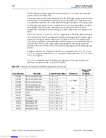
The board utilizes the EPM2210 System Controller, an Altera MAX
II CPLD, for the
following purposes:
■
FPGA configuration from flash memory
■
Power consumption monitoring
■
Virtual JTAG interface for PC-based GUI
■
Control registers for clocks
■
Control registers for remote system update
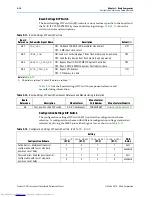
Figure 2–3
illustrates the MAX II CPLD EPM2210 System Controller's functionality
and external circuit connections as a block diagram.
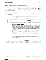
Table 2–5
lists the I/O signals present on the MAX
II CPLD EPM2210 System
Controller. The signal names and functions are relative to the MAX
II device (U10).
Figure 2–3.
MAX II CPLD EPM2210 System Controller Block Diagram
Information
Register
MAX II
Embedded
USB-Blaster
MAX II CPLD EPM2210 System Controller
Power
Calculations
SLD-HUB
PFL
Power
Measurement
Results
Virtual-JTAG
PC
EP4CGX15
LTC2418
Controller
FLASH
Decoder
Encoder
JTAG Control
SSRAM
Control
Register
LCD
GPIO
Table 2–5.
MAX II CPLD EPM2210 System Controller Device Pin-Out (Part 1 of 3)
Schematic Signal Name
I/O
Standard
EPM2210
Pin Number
EP4CGX15BF14
Pin Number
Description
CLK125_EN
2.5-V
R1
—
125-MHz oscillator enable
CLK125_SDA
T2
—
125-MHz programming data
CLK125_SCK
R3
—
125-MHz programming clock
CLK_SEL
R4
—
DIP - clock select SMA or oscillator
CLK_MAXII
J5
—
MAX II clock input
EPCS_nCS
B13
C5
EPCS memory chip enable
FLASH_CEn
A2
B8
FSML bus flash memory chip enable
FSML_OEn
B1
B13
FSML bus flash memory output enable
electronic components distributor


