HR-16/HR16B Service Manual 1.00
1
1.0 General Description
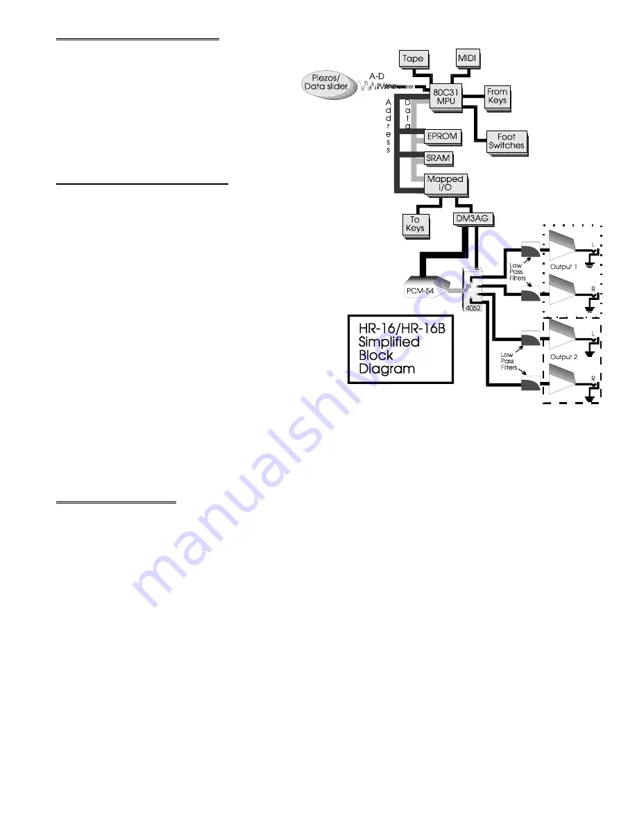
Diagram 1 provides a simplified
block diagram to show major sub
systems. Note that the schematic
reference designations and pinouts
used in this manual refer to the AQ
revision of both the main PCB, and
schematic.
1.1 Main PC Board Revisions
There are 3 major main PC
Board revisions.
•
A-This was the initial release. This
board revision will require the most
extensive updating of the three.
•
CA-This version of the board was a
4 layer design. While offering
several advantages over the older
version (improved R.F.
characteristics, smaller size, etc.) it
was found to be extremely difficult to
service (internal shorts can only be
repaired using lifted pins and
jumpers).
•
AQ-This was the final revision. This
revision will of course need the
fewest updates, and should be
relatively easy to troubleshoot.
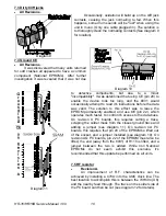
Diagram 2 is provided in order to assist with board revision identification.
2.0 Power Supply
The power supply begins with the 9 Volt A.C., adapter (Alesis P2 [mini plug] or P3 [barrel]
types). Input from J1 is R.F. filtered before on/off switch S1. From there it is split for the +12V, -12V,
and +5V rails. The +12V rail consists of a voltage doubler (C1, C3, and D2, D3), a 7812 regulator
(U8), and a filter capacitor (C6). The -12V rail is a "mirror" of the +12V rail, consisting of voltage
doubler (C2, C4, and D1, D4), a 7912 regulator (U9), and a filter capacitor (C7). The +5V rail
consists of a rectifier diode (D5), a filter capacitor (C5), a 7805 regulator (U10), and a multitude of
0.1
µ
F bypass capacitors. Note that the raw +10V line used by the microprocessor reset, and the
SRAM power supply (when retrofitted), is located at the input to the 7805 regulator. Note that
revision AQ (the latest) boards also incorporate several R.F. suppression chokes and current
limiting resistors. These have resulted in a few unique situations that may need to be dealt with (see
section 7.16 for details)
Diagram 1


