background image

12

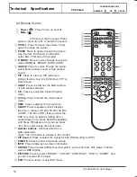
4.4 Remote Control


Power (   )

: Press to turn on and off.


Mute ( 

 )

: Press to mute the sound. Press  

    again or press ◄ or ► to restore the sound.


P.STILL

: Press to freeze the picture. Press  

    again to restore the picture. 


P.SIZE

: Press to cycles through the picture  

    size: Normal, Fill Screen, Anamorphic, 

    Letter Box, TV Mode or Panorama. 


P. MODE

: Press to cycles through the picture

     mode: NORMAL, BRIGHT, DARK, USER. 


S.SELE

: Press to cycles through the sound 

    select: Main window sound or Sub window  

    sound.


PIP

: Press to turns on PIP (picture-in-

    picture) feature. Such as Full Screen, PIP or  

    Split Screen.


SWAP

: Press to switches the Main window  

    or Sub window pictures.


C/C

: Press to select the Closed Caption    

    mode.


  V-Chip

: Press to select the child protect    

    mode.


  TIME

: Press to display the current time.


SLEEP

: Press repeatedly until it displays  

    the time in minutes (30 Min, 60 Min, 90 Min,  

    120 Min, 180 Min or Off ) that you want the  

    PDP to remain on before shutting off. To  

    cancel Sleep Time, press SLEEP repeatedly  

    until Sleep Off appears. And you can press   

    ◄ or ► to select sleep time shut down.


Number buttons

: Use these buttons to 

    enter password. 


(Note: The 100 button is inactive in this model.)


  PIP Source

: Press to select the signal for Sub Window.(Only for PIP.)


F.WHITE

: Press to show a full white picture.


INFO

: Press to display on-screen information. 


SOUND

: Press to select different sound system, such as Normal, Flat, News, Cinema,   

    User or BBE Digital.


PICTURE

: Press to select “BRIGHT”, “COLOR”, “CONTRAST”, ”HUE” or “SHARP”, and  

    you can use◄ or ► to adjust.


EXIT

: Press to return or exit OSD menu.


(Continued on next page)


REMOTE CONTROL

CONTINUATION PAGE 

Technical  Specifications                 

PDP-50

0

6

H

NUMBER     

8     

OF  

9


 PAGES 

Summary of Contents for PDP5006H

Page 1: ...cuit Description Main IC Specifications Trouble Shooting Manual of PDP Module Spare Part list Exploded View If You Forget Your V CHIP Password Software Upgrade This manual is the latest at the time of...

Page 2: ...k of electric shock to persons The exclamation point within an equilateral triangle is intended to alert the user to the presence of important operating and maintenance servicing instructions in the l...

Page 3: ...way from high voltage or high tempera ture components 8 Before returning the set to the customer always perform an AC leakage current check on the exposed metallic parts of the cabinet such as antenna...

Page 4: ...ER OF PAGES 9 REVISIONS ISSUED DATE DESCRIPTION RAISED BY SPECIFICATION AGREED SIGNATURE DATE R D DEPARTMENT COMMERCIAL DEPARTMENT PRODUCTION DEPARTMENT Q A DEPARTMENT CUSTOMER SPECIFICATION APPROVED...

Page 5: ...0 photometer 1 6 Magnetic field no restricted 1 7 Control settings Brightness Contrast Tint Color set at Center 50 1 8 Power input 100 240Vac 1 9 Ambient temperature 20 C 5 C 68 F 9 F 1 10 Display mod...

Page 6: ...2 7 Withstanding voltage 1 5kVac or 2 2kVdc for 1 sec 3 Display 3 1 Screen Size 50 Plasma display 3 2 Aspect Ratio 16 9 3 3 Pixel Resolution 1366x768 3 4 Peak Brightness 1000 cd m Panel module withou...

Page 7: ...sport 5 2 1 Temperature 20 C to 60 C 4 to 140 F 5 2 2 Relative humidity 5 to 95 6 Panel Characteristics 6 1 Type S50HW XD03 6 2 Size 50 1190mm width x7005mm height x59mm depth 1 mm 6 3 Aspect ratio 16...

Page 8: ...ush the key to select the input signals source 7 2 Stand by Button Switch on main power or switch off to enter power Saving modes 7 3 Main Power Switch Turn on or off the unit 8 OSD Function 8 1 Pictu...

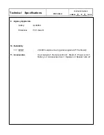
Page 9: ...ES 9 Agency Approvals Safety UL60950 Emissions FCC class B 10 Reliability 11 1 MTBF 20 000 hours Use moving picture signal at 25 C ambient 11 Accessories User manual x1 Remote control x1 Stand x1 Powe...

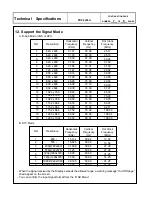
Page 10: ...0 24 31 50 31 50 28 32 36 00 40 00 49 50 50 00 57 27 65 00 75 00 78 75 80 37 94 51 108 03 108 04 108 00 1152 x 864 1152 x 864 1 2 3 5 6 7 8 9 10 11 12 13 14 15 16 17 18 19 4 12 Support the Signal Mode...

Page 11: ...otect mode TIME Press to display the current time SLEEP Press repeatedly until it displays the time in minutes 30 Min 60 Min 90 Min 120 Min 180 Min or Off that you want the PDP to remain on before shu...

Page 12: ...uttons in the OSD Menu screen and they can be used for the selection of the program when the OSD Menu is not shown on the screen They are used as buttons in the OSD Menu screen and they can be used fo...

Page 13: ...mmon sustain driver Display data Driver timing Memory Controller Driver Timing Controller Input Interface Controller Vcc 5V Va 55V 65V Vs 180V 190V Control Signal Serial Interface APL Data LVDS Input...

Page 14: ...e Interlacer YCrCb DVI Tuner x 2 SCART1 Sil161B DVI Receiver MSP34x0G Audio Decoder AD9883A ADC VPC3230D Vide Decoder TDA8946 Audio AMP S Video YPbPr Video2 Speaker M52790 A V Switch uPD64083 3D Y C S...

Page 15: ...Circuit Diagram Power supply board of Audio Amplifier MPT012A Main Video board Sub Audio board Keypad board Remote control receiver board Remote control board...

Page 16: ......

Page 17: ......

Page 18: ...DbhM4812V12_Vtek_BOM sch 3 Wed Oct 06 23 58 10 2004...

Page 19: ...DbhM4812V12_Vtek_BOM sch 4 Wed Oct 06 23 58 11 2004...

Page 20: ...DbhM4812V12_Vtek_BOM sch 5 Wed Oct 06 23 58 15 2004...

Page 21: ...DbhM4812V12_Vtek_BOM sch 6 Wed Oct 06 23 58 16 2004...

Page 22: ...DbhM4812V12_Vtek_BOM sch 7 Wed Oct 06 23 58 18 2004...

Page 23: ...DbhM4812V12_Vtek_BOM sch 8 Wed Oct 06 23 58 29 2004...

Page 24: ...DbhM4812V12_Vtek_BOM sch 9 Wed Oct 06 23 58 20 2004...

Page 25: ...DbhM4812V12_Vtek_BOM sch 10 Wed Oct 06 23 58 22 2004...

Page 26: ...DbhM4812V12_Vtek_BOM sch 11 Wed Oct 06 23 58 32 2004...

Page 27: ...DbhM4812V12_Vtek_BOM sch 12 Wed Oct 06 23 58 25 2004...

Page 28: ...DbhM4812V12_Vtek_BOM sch 13 Wed Oct 06 23 58 27 2004...

Page 29: ...Dbh1S4909V12 sch 2 Thu Oct 07 00 30 42 2004...

Page 30: ...Dbh1S4909V12 sch 3 Thu Oct 07 00 30 43 2004...

Page 31: ...Dbh1S4909V12 sch 4 Thu Oct 07 00 30 45 2004...

Page 32: ...Dbh1S4909V12 sch 5 Thu Oct 07 00 30 47 2004...

Page 33: ...Dbh1S4909V12 sch 6 Thu Oct 07 00 30 49 2004...

Page 34: ...Dbh1S4909V12 sch 7 Thu Oct 07 00 30 50 2004...

Page 35: ...Dbh2S4909V12 sch 2 Thu Oct 07 00 32 34 2004...

Page 36: ...DUBHE OSD Ver1 1_NAKS sch 1 Mon Oct 18 11 47 11 2004...

Page 37: ...0025 sch 1 Mon Sep 05 15 03 59 2005...

Page 38: ...c s Y Z Sustainer board 2 pc s Y Drive board 6 pc s X Extension boards 1 pc Control Signal Input and 1 pc Power board in the Module SET There are 6 pc s PCBs including 1 pc AUX PSU Board 1 pc Keypad b...

Page 39: ......

Page 40: ...ital ones and to transmit to Control board 3 Control board Dealing with the digital signal LVDS for output to panel 4 Y Sustainer Z Sustainer board 1 Receiving the signals from Control and high voltag...

Page 41: ...o picture but with signals output OSD and back light d Abnormal noise on screen 3 POWER No picture no power output 4 Z Sustainer a No picture b Color not enough c Flash on screen 5 Y Sustainer Darker...

Page 42: ...cro Processor will send on control signal to power Then Power sends 5Vsc 9Vsc 24V and RLYON Vs ON to PCBs working This time Main will send signals to display Image OSD on the panel and start to search...

Page 43: ...Video Signal Processor uPD64083 Three Dimensional Y C Separation LSI With On Chip Memory AD9883A 110MSPS 140MSPS Analog Interface VPC 323XD Comb filter Video Processor Si161B Panel Link Receiver Z8622...

Page 44: ...ffer including motion adaptive temporal deinterlacing with film mode detection When used in combination with the new third generation scaler this advanced video processing technology delivers the high...

Page 45: ...The AD9883A is a complete 8 bit 140 MSPS monolithic analog interface optimized for capturing RGB graphics signals from personal computers and workstations Its 140 MSPS encode rate capability and full...

Page 46: ...This high level of integration enables simple flexible cost effective solutions that require fewer components Features Built In Memory Controller Motion Adaptive Deinterlace Processor Intelligent Edg...

Page 47: ...es the Wide Clear Vision ID signal Japanese local format decoder and ID 1 signal decoder FEATURES On chip 4 Mbit frame delay memory 4 Operation mode Compatible to the PD64082 Motion adaptive 3D Y C se...

Page 48: ...656 output interface peaking contrast brightness color saturation and tint for RGB YCrCb and CVBS S VHS high quality soft mixer controlled by Fast Blank PIP processing for four picture sizes or of nor...

Page 49: ...logy simplifies PC and display interface design by resolving many of the system level issues associated with high speed mixed signal design providing the system designer with a digital interface solut...

Page 50: ...application The robust nature of the Z86229 helps the device conform to the transmissionformat defined in the Television Decoder Circuits Act of 1990 and in accordance with the Electronics Industry As...

Page 51: ...for BTSC and EIA J The MSP 34x0G has optimum stereo perfor mance without any adjustments All MSP 34xxG versions are pin compatible to the MSP 34xxD Only minor modifications are necessary to adapt a M...

Page 52: ...MODEL 50 HD D3 1 PDP 1 269cm 50 Inch Wide Plasma Display Module Quality Innovation Team 1 37...

Page 53: ...on of a electrical shock measure against power outage etc 3 Name Function 3 1 Layout of Assemblies 3 2 Block Diagram 3 3 Main function of Each Assembly 3 4 Product Serial Label Location 4 Operation ch...

Page 54: ...Samsung SDI Co Ltd A S Manual Plasma Display Module 1 Overview 1 1 Model Name of Plasma Display MODEL 50HD D3 1 PDP S50HW XD03 1 2 External View M3 X Board Y Board Logic Board PSU SUB PSU 3 37...

Page 55: ...Samsung SDI Co Ltd A S Manual Plasma Display Module 1 3 Points of Screw Mount Blue Dot SCREW 4X12 Red Dot SCREW 3X10 4 37...

Page 56: ...ize Horizontal 1106 46 Vertical 622 08 6 Screen size Diagonal 50 Color Plasma Display Module 7 Screen aspect 16 9 8 Display color 16 77 million colors 9 Viewing angle Over 160 Angle with 50 and greate...

Page 57: ...t place The capacitor s remaining voltage in the PDP module s circuit board temporarily remains after power is off Operator must wait for discharging of remaining voltage during at least 1 minute PDP...

Page 58: ...t change the electrical circuit design For example Do not insert a subsidiary audio or video connector If you insert It It cause danger on safety And If you change the design or insert Manufactor guar...

Page 59: ...ic which can charge a enough positive electric enough damaging ESD Before removeing the protective material from the lead of a new ESD bring the protective material into contact with the chassis or as...

Page 60: ...Samsung SDI Co Ltd A S Manual Plasma Display Module 3 NAME FUNCTION 9 37 3 1 Layout of Assemblies 20 26 35 27 28 32 10 9 11 12 33 34 2 1 5 14 15 4 30 3 13 6 7 8 24 21 22 19 16 18 17 29 31 23 25...

Page 61: ...PCB BUFFER 16 3809 001526 LOGIC Y MAIN FFC CABLE FLAT 17 3809 001516 LOGIC X MAIN FFC CABLE FLAT 18 3809 001414 SUB R LOGIC FFC CABLE FLAT 19 3809 001414 SUB L LOGIC FFC CABLE FLAT 20 3809 001414 LOGI...

Page 62: ...Samsung SDI Co Ltd A S Manual Plasma Display Module 1 L Main 2 X Main 8 I Buffer 3 Y Main 3 E Buffer 4 F Buffer 5 G Buffer 7 H Buffer 11 37...

Page 63: ...Samsung SDI Co Ltd A S Manual Plasma Display Module 9 J Buffer 10 Y Buffer lower 11 Y Buffer Down 12 Sub R 13 Sub L 3 2 BLOCK DIAGRAM 3 2 1 BLOCK DIAGRAM FOR DRIVE CIRCUIT OPERATION 12 37...

Page 64: ...Column Driver Vsc_l Display Data LOGIC CONTROL DRIVER CIRCUIT PANEL 3 3 Main function of Each Assembly X main board The X main board generate a drive signal by switching the FET in synchronization wi...

Page 65: ...and control signal Y buffer board Upper Lower The Y buffer board consisting of the upper and lower boards supplies the Y terminal with scan waveforms The board comprises 8 scan driver IC s ST microele...

Page 66: ...anel module label 3 4 1 Serial No 2 6 1 4 0 8 07 0 8 6 5 Serial No 0001 9999 Date 01 31 Month 01 12 Year 00 2000 99 2099 Line No 1 9 0 Pilot Line Type 02 48 ex 50HDv3 26 Step of even 15 37 3 4 PRODUCT...

Page 67: ...V 3 Adjusting the output signal through test points 4 Checking the panel s crack 4 1 1 No voltage output 16 37 Check LED 8001 8002 Green NG PSU Voltage check D5V 5V Check Vs 170V Check Va 72V Check Vs...

Page 68: ...Vs_on Check output voltage Vs Va Vset Vscan Ve NG Replace PSU Turn off Relay SW Open these connector One by One CN8002 X Main check CN8003 Y Main check CN8005 CN8006 Buffer check OK Replace PSU If LED...

Page 69: ...he following pages show you how to find the defective board No Display Logic Main Vsync Blinks LED 1 Y Main Broken panel Logic B d NG OK Y Main NG OK Fuse OPEN OK FET SHORT X Main Replace Logic B d Ch...

Page 70: ...4021 Q4013 Q4019 Q4006 Q4020 Q4009 Q4010 Q4022 Q4014 Q4015 Q4016 Q4017 Q4023 4 1 3 Abnormal Display Abnormal Image is on Screen except abnormality in Sustain or Address Abnormal Display is related wit...

Page 71: ...0V OPEN Fuse Replace Y B d OK SHORT FET Check Q5007 Q502 Q5011 Q50112 Q5027 Q5009 Q5008 Q5030 Q5013 Q5014 Q5029 Q5018 Q5019 Q5028 Replace Y B d OK X Main OK OPEN Fuse Replace X B d OK Check Q4004 Q400...

Page 72: ...ogic Main Vsync Blinks LED 1 Motion of Vsync Regular Abnormal OK Replace board NG Logic main Normal State 4 1 4 Sustain Open some horizontal lines don t exist on screen Y FPC Sustain Open After Changi...

Page 73: ...ines don t exist on screen Address Open is related with Logic Main Logic Buffer FFC TCP and so on This page shows you how to check the boards and the following pages show you how to find the defective...

Page 74: ...e PDP NG 4 1 7 Address Short some vertical lines appear to be linked on screen Address Short is related with Logic Main Logic Buffer FFC TCP and so on This page shows you how to check the boards and t...

Page 75: ...bnormal Image not open or short is on screen Y MAIN X MAIN Logic Main Sustain Open some horizontal lines don t exist on screen Scan Buffer FPC of X Y Sustain Short some horizontal lines appear to be l...

Page 76: ...e manufacturing Panel electrode single line foreign material electrostatic TCP defect Parts TCP Board connection defect Operation Assembly error Film damage Symptom Another color simultaneously appear...

Page 77: ...tom A defect other than address open and short Data printout signal error occurring at certain Gradation or pattern Symptom One or more line do not light up in Sustain direction Cause manufacturing Pa...

Page 78: ...or low gradation patter Cause manufacturing Panel electrode short Foreign material Parts Board connector pin error Operation connector assembling error Symptom Burn caused by the damage of address bus...

Page 79: ...r normal temparature Cause Panel MgO source dielectric thickness cell pitch phosphor Circuit drive waveform voltage condition Symptom Normal discharge but cells appear darker due to weak light emissio...

Page 80: ...g on the damaged parts and damage level Cause Manufacturing Flatness palette pin interruption Operation overload of panel corner careless handling Panel Flatness assembly error Symptom Crack in break...

Page 81: ...potentiometer 5 Dummy Discharge Resistor 2 4kOhm 10W 5 1 2 Measuring Equipment 1 Oscilloscope 500MHz sampling 2 Probe 10 1 3 Digital Multi meter 4 Signal Generator 5 3 Disassembling Re assembling 5 3...

Page 82: ...connector pin during connecting by mistake 5 3 2 Assembling Disassembling of Flat Cable Connector of X Main Board 1 Disassembling Procedure 1 Pull out the clamp of connector 2 Pull Flat cable out pre...

Page 83: ...the TCP out from Connector 2 Assembling of TCP 1 Put the TCP into the Connector carefully 2 Close the clamp completely The sound Dack comes out Notice TCP and Connector was connected surely Notice 1 C...

Page 84: ...ung SDI Co Ltd A S Manual Plasma Display Module 3 Misassembling of TCP 1 The misassembling of TCP is the cause of defect 4 Checking method of misassembling of TCP 1 5 Assembling Disassembling of FFC 3...

Page 85: ...SDI Co Ltd A S Manual Plasma Display Module This is the photo of the assembling of FFC The procedure of assembling and disassembling of FFC is the same as TCP 5 3 4 Exchange of LBE LBF LBG board Photo...

Page 86: ...tightly 6 Get rid of the foreign material from the connector 7 Connect the TCP FFC and power cable to the connector 8 Reassemble the TCP heat sink 9 Screw in order of Right Side Left Side Center Photo...

Page 87: ...fected board 8 Reassemble the YBU and YBL to the Y Main 9 Connect the connector of CN5006 and CN5007 among YBU YBL and YM 10 Arrange the board on the chassis and then screw to fix 11 Connect the FPC a...

Page 88: ...ch is setting SW2000 3 Turn on the power to PDP module and then check that LED lights up and the SET is working well 4 Check the power voltage after turn on the power and then check the Display condit...

Page 89: ...2D1 PCS 4 269 42D101 01L REMOTE LENS 42D1 PCS 5 322 42P101 01 REMOTE LENS RUBBER SPACER PDP 42TP1 PCS 6 322 42P102 01 POWER LENS RUBBER SPACER PDP 42TP1 PCS 7 322 42P103 01 SEPARATE RUBBER SPACER FOR...

Page 90: ...GASKET 200X9X4 0MM W CONDUCTI PCS 50 553 024509 40A SHIELD GASKET 245X9X4 0MM W CONDUCTI PCS 51 553 026009 40A EMI SHIELD GASKET 260X9X4 0MM W COND PCS 52 553 028009 40A EMI SHIELD GASKET 280X9X4 0MM...

Page 91: ...0AD02 01 WOOD PALLET 1545X745X116 PCS 84 900 50AA01 01 DISPLAY FILTER 50 OPTIMAX FOR SAMSU PCS PACKING 1 300 50P101 02C POLYFOAM TOP 50TP1 PCS 2 300 50P102 02C POLYFOAM BOTTOM 50TP1 PCS 3 310 111404 0...

Page 92: ......

Page 93: ...ect the RS 232C input jack to an external control device such as a computer and software upgrade Type of connector D Sub 9 pin male 1 No Pin name 5 1 No connection 2 RXD Receive data 3 TXD Transmit da...

Page 94: ...ter Open the software Flash Upgrader exe Point Flash on the interface of the Flash Upgrader exe Press STANDBY button on the front panel or POWER button of Remote control Power indicator green the PDP...

Reviews: