27
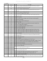
1
DEFI
I
Defect detection signal (DEF) input. ("L" is applied when not used.)
2
TAI
I
For PLL/Test input. (Connected to 0V)
3
PDO
O
Phase comparison output to control the external VCO.
4
VVSS
Ground of the built-in VCO. Normally 0V.
5
ISET
I
For the connection of a resistor which adjusts the PDO output current.
6
VVDD
Power supply of the built-in VCO.
7
FR
I
Adjusts the VCO frequency range.
8
VSS
Ground of digital circuits. Normally 0V.
9
EFMO
O
For slice level control/EFM signal output.
10
EFMIN
I
EFM signal input.
11
T2
I
Test input. A pull-down resistor is incorporated. (Connected to 0V)
12
CLV+
O
Disc motor control tri-state output.
13
CLV-
14
V/PO
Output to monitor the automatic switching between the rough servo control and phase servo
control. "H" : Rough servo, "L": Phase servo.
15
HFL
I
Track detection signal input. Schmitt trigger input.
16
TES
I
Track error signal input. Schmitt trigger input.
17
TOFF
O
Tracking off output.
18
TGL
O
Tracking gain switching output. "L" raises the gain.
19
JP+
O
Track jump control tri-state output.
20
JP-
21
PCK
O
Monitors the clock signal for EFM data playback. 4.3218MHz when the phase is locked.
(Not used)
22
FSEQ
O
Sync signal detection output. Goes "H" when the sync signal detected from the EFM
signal matches the sync signal generated internally. (Not used)
23
VDD
Power supply of digital circuits.
24
SL+
O
Controlled by serial data command issued by the microprocessor.
25
SL
O
Controlled by serial data command issued by the microprocessor.
26
V/P MONI
I
Prevent high speed rotation of no recording CD-R/RW disc by watch V/P.
27
SW-INSIDE
I
CD pickup inside limit switch.
28
CD R/W
O
CD-RW disc select control.
29
EMPH
O
Deemphasis monitor. "H": when playing a deemphasis disc. (Not used)
30
C2F
O
C2 flag output. (Not used)
31
DOUT
O
Output a digital OUT signal. (EIAJ format)
32
T3
I
Test input. (Connected to 0V)
33
T4
34
PCCL
Not used.
35
MUTE-L
O
Lch 1-bit DAC/Lch muting output. (Not used)
36
LVDD
Lch power supply.
37
O-LCH
O
Lch output.
38
LVSS
Lch ground. Normally 0V.
39
RVSS
Rch 1-bit DAC/Rch ground. Normally 0V.
Description
Pin No.
Pin Name
I/O
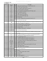
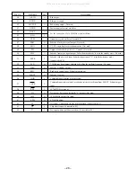
IC DESCRIPTION
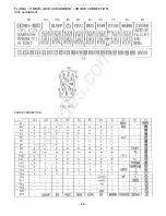
IC, LC78622NE
All manuals and user guides at all-guides.com
Summary of Contents for XR-EM70
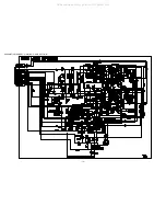
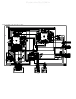
Page 13: ...13 SCHEMATIC DIAGRAM 2 MAIN 2 2 AMP SECTION All manuals and user guides at all guides com...
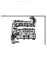
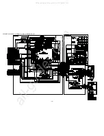
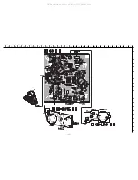
Page 18: ...18 SCHEMATIC DIAGRAM 4 CD CD DRIVE CD LOAD All manuals and user guides at all guides com...
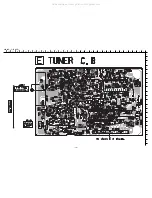
Page 20: ...20 SCHEMATIC DIAGRAM 5 TUNER All manuals and user guides at all guides com...
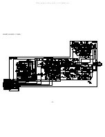
Page 22: ...22 SCHEMATIC DIAGRAM 6 PT All manuals and user guides at all guides com...
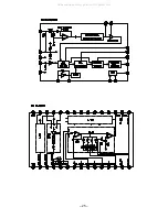
Page 24: ...24 IC BLOCK DIAGRAM All manuals and user guides at all guides com...
Page 25: ...25 All manuals and user guides at all guides com...

