– 43 –
< TUNER SECTION >
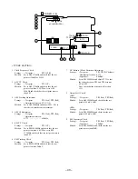
1. Clock Frequency Check
Settings :
• Test point :
TP2 (CLK)
Method :
Set to AM 1710kHz and check that the test
point is 2160kHz
±
45Hz.
2. AM VT Check
Settings :
• Test point :
TP1 (VT)
Method :
Set to AM 1710kHz and check that the test
point is less than 8.5V. Then set to AM
530kHz and check that the test point is more
than 0.6V.
3. AM Tracking Adjustment
Settings :
• Test point :
TP8 (Lch), TP9 (Rch)
• Adjustment location : L981 (1/3)
Method :
Set to AM 1000kHz and adjust L981 (1/3) so
that the test point becomes maximum.
4. AM IF Adjustment
Settings :
• Test point :
TP8 (Lch), TP9 (Rch)
• Adjustment location :
L772 ........................... 450kHz
5. FM VT Check
Settings :
• Test point :
TP1 (VT)
Method :
Set to FM 108.0MHz and check that the test
point is less than 8.0V. Then set to FM
87.5MHz and check that the test point is more
than 0.5V.
6. FM Tracking Check
Settings :
• Test point :
TP8 (Lch), TP9 (Rch)
Method :
Set to FM 98.0MHz and check that the test
point is less than 9dB
µ
V.
7. DC Balance / Mono Distortion Adjustment
Settings :
• Test point :
TP3,TP4 (DC balance)
• Adjustment location : L771
• Input level :
60dB
µ
V
Method :
Set to FM 98.0MHz and adjust L771 so that
the voltage between TP3 and TP4 becomes
0V
±
0.04V.
Next, check that the distortion is less than
1.3%.
8. Output Level Check
<AM>
Settings :
• Test point :
TP8 (Lch), TP9 (Rch)
Method :
Set to AM 1000kHz and check that the test
point is 130mV
±
3dB.
<FM>
Settings :
• Test point :
TP8 (Lch), TP9 (Rch)
Method :
Set to FM 98.0MHz and check that the test
point is 520mV
±
3dB.
9. FM Separation Check
Settings :
• Test point :
TP8 (Lch), TP9 (Rch)
• Input level :
60dB
µ
V
Method :
Set to FM 98.0MHz and check that the test
point is more than 25dB.
L771
L981
L772
FFE801
TP5(STOP)
1
IC771
TP1(VT)
TP2(CLK)
TP4(DC)
TP3(DC)
1
CN701
(GND)
TP8
(LCH)
TP9
(RCH)
TUNER C.B
Q
1
2
3
3
4
4
5
6
8
9
7
7
Summary of Contents for XH-N5
Page 15: ... 15 FL BJ741GK GRID ASSIGNMENT ANODE CONNECTION GRID ASSIGNMENT ...
Page 16: ... 16 ANODE CONNECTION ...
Page 18: ... 18 SCHEMATIC DIAGRAM 1 MAIN 1 2 FUNCTION BBE DSP ECHO CONNECT1 3 ...
Page 19: ... 19 SCHEMATIC DIAGRAM 2 MAIN 2 2 DECK ...
Page 21: ... 21 SCHEMATIC DIAGRAM 3 FRONT DECK DECK MOTOR CONNECT2 3 ...
Page 23: ... 23 SCHEMATIC DIAGRAM 4 OPERATE KEY MIC LED A LED B LED C LED D ...
Page 25: ... 25 SCHEMATIC DIAGRAM 5 AMP AMP C B ...
Page 27: ... 27 SCHEMATIC DIAGRAM 6 VIDEO I O VIDEO JACK VIDEO 3 CONNECT 3 3 ...
Page 28: ... 29 SCHEMATIC DIAGRAM 7 TUNER ...
Page 30: ... 31 SCHEMATIC DIAGRAM 8 PT VOLTAGE SEL SW ...
Page 32: ... 33 IC BLOCK DIAGRAM IC BU4052BCF IC BA7625 ...
Page 33: ... 34 IC BU4094BCF IC BA7762AFS ...
Page 34: ... 35 IC M62445AFP IC SPS 442 1 F ...
Page 35: ... 36 IC BA3880FS IC LC72131D ...
Page 36: ... 37 IC BA3835F IC LA1837NL ...
Page 37: ... 38 IC BU2099FV IC BU9262AFS ...


