


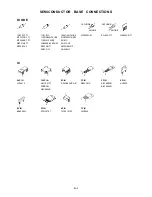


PRINTED WIRING BOARDS
SYSCON
I-5
A
B
C
D
E
F
A
B
C
D
E
F
1
2
3
4
5
1
2
3
4
5
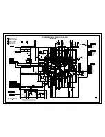
TU601
CP4001_1
CP4004
W148
L4001
L4005
Q4002
W225
W149
W150
D4003
W141
W139
W138
C4042
C4040
C4038
C351_1
C4049
L4012
C4051
C4039
C4041
C4025
C4036
C4057
L4011
C4069
C4050
TP4002
TP4001
W311
C4088
C4078
C4074
C4073
C4071
C4055
W147
W145
W216
C4091
C4064
W146
W151
L4016
W144
W829
W087
C4084
C4102
Q4001
W905
W210
W116
W085
W081
W079
R674
R673
R4041
CP603
J4501
HS351
IC352
R4040
C4080
R605
W174
X4001
Q1017
CP502
W292
CD810
IC1003
W291
R1068
R1073
R1085
C1037
R1036
IC1004
C1045_1
W287
D1019
C1036
R658
W310
W294
W250
W251
W295
W248
IC1005
HS1001
C1029_1
R1069
Q1010
C1033
W253
W309
W293
R355
W214
W211
W213
C357
W296
W227
R308
W231
C358_2
W229
W878
C354
W830
C352
R353
C4024
W212
W142
W088
W011
W016
C882
W115
C611
C613
C612
W029
W013
W108
W893
C883
W080
W117
R1016
Q1001
D852
D1003
C881
W002
R4028
W001
W012
W004
W015
SW1001
CP351
W069
W070
W071
W109
W010
W030
W246
W222
W252
W243
W166
W168
W163
W164
W157
W096
W095
W091
W196
W190
W187
W179
W032
W201
W202
W136
W195
D1008
R1086
W090
W046
W048
W049
W064
W038
W054
W053
W052
W051
R1018
W055
W035
W033
W039
W040
W034
W060
W059
W045
W043
W089
W017
W050
W057
W061
W056
W065
W044
W037
W036
W130
W127
R1014
C1048
W137
W063
R1050
C1032
R1079
L1001
W123
C1020
C1013
W122
Q1005
Q1009
Q1003
D1017
C1001
X1002
D1010
D1006
D1005
X1001
W207
D1004
D1001
R1003
TP1001
W058
R1056
R1006
W186
Q4005
Q4004
IC1001
IC1002
D1002
C1003
C1021
IC1099
R1019
C
P1
004
W193
D1014
D1015
D1016
D1012
W194
W192
W198
W156
W155
W160
W241
W158
W161
W199
W200
W857
W822
W825
W134
W062
W828
CP757_1
W245
W233
W112
W132
W152
W114
W105
W113
W106
W118
W072
W119
W815
W074
W162
W075
W076
W110
W025
W024
W022
W026
W124
D1009
W191
W180
W121
W125
W279
W280
W281
W267
W270
W318
W317
W254
R4008
W308
W307
D604
W817
R4507
W263
C675
W316
R4539
W303
W313
CD850
W315
W312
W314
C642
R656
W272
W326
L4008
D4510
W333
CF601
W321
C4522
W276
R666
D601
W324
W843
TP4501
L4504
X601
C667
R615
W332
C634
L603
R604
C605
W271
W269
W331
W298
W301
W300
W299
C645
W240
CF602
IC601
L608
L601
L609
C652
C651
C620
C626
C622
C618
C659
C4508
L4503
C4509
C656
C658
L604
Q601
L606
W262
W182
W854
W018
W807
W006
R1101
D4202
W027
W028
W023
R620
W103
R1031
W042
W094
W131
W197
W185
W073
W021
W098
W102
W172
L4502
C1070
W203
W208
Q1018
C1102
L4004
W126
W128
W101
W041
W129
W047
C4001
W256
W812
C1016
W206
W209
W205
W120
C4015
C4017
HS1002
W285
C1042_1
W289
W286
W290
R1081
C636_1
L4007
L4013
L4002
L4015
L4009
L605
L4003
L4006
W140
C4108
W856
W304
W340
W306
W173
W066
W067
CD653
W302
W226
W819
W219
W220
W215
W167
W336
D1022
W099
W100
W097
R1002
W005
W019
W020
W339
W175
W184
W188
W337
W342
W334
W305
D1018
W232
W347
W346
Q1019
W288
D606
D4503
D605
W804
W320
W154
W153
W165
R654
W265
W268
W322
W275
W228
C632
W351
W353
W171
W170
W352
W349
W093
W350
W348
W354
CP1005_1
CP1006
CP4005
CP302_1
W355
C628
C1064
R1005
B4503
C614
C4031
C4009
C616
Q608
B4504
D608
D609
D610
R651
W111
C359
W931
W934
R1047
D350
D611
D612
C4504
W861
C639_1
W183
W357
W247
W244
W242
W360
R650
C617
W872
C669
W031
W802
W806
R4511
W875
W907
W841
W924
W867
W846
W910
D1023
S804X
S804Y
R681
R1054
R1052
W876
R350
S111X
S111Y
S802X
S802Y
C1083
CD652
C1084
D1024


